


 HOME
HOME


"Thin Film Ceramic PCB" technology distinguishes itself by employing a metal deposition method using vacuum processes, granting it unparalleled flexibility in thickness and metallization type. This sets it apart from conventional printed circuit board technology, where limitations exist in terms of flexibility and conductor geometries. By enabling extreme connection densities and precise conductor geometries, thin-film ceramic circuit has become the go-to solution for high-performance applications where intricate designs are paramount.
Thin-film technology's potential for higher track resolution is one of its key assets, enabling engineers to achieve significantly increased interconnection density. This translates to better connectivity and improved signal performance compared to thick-film or LTCC (Low-Temperature Co-fired Ceramic) alternatives. Thin film ceramic PCB always be chosen for specialized applications where cheaper alternatives fall short. With higher track resolution, it excels in telecommunications and diverse industries, including extreme thermal and biomedical applications. Future prospects involve nanotechnology integration, three-dimensional circuits, and eco-friendly aspects.
-
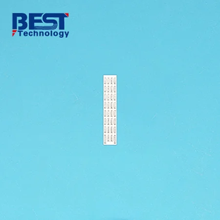
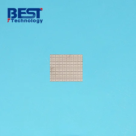
Thin-film Ceramic Circuit Board Rapid Prototype For Energy Storage System
-
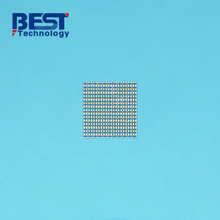
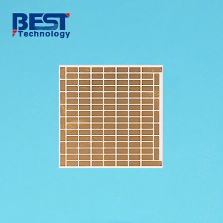
Soul Ultra-thin Film Ceramic PCB Design For Robot Control System
-
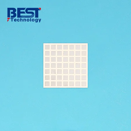
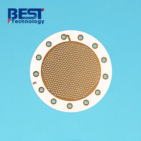
Thin-film Ceramic PCB Fast Turn Assembly For Radar Control System
-
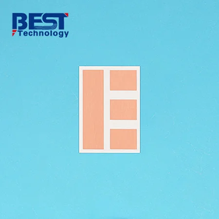
Thin Film Circuit Board Design Production For New Energy System
-
Ultra-thin Ceramic Substrate Thin Film PCB For Vehicle Driving Control System
-
Thin Film Ceramic Circuit Board Medical Equipment Application
-
Thin film ceramic PCB Design Fabrication For Wireless Communication
 Products
 About us
 Contact us


