


 HOME
HOMEApplications of Ceramic Circuit Boards
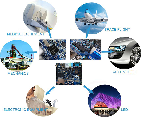
Applications of Ceramic Circuit Boards
Ceramic circuit boards are popular for their excellent performance than normal FR4 PCB or Metal core PCB, especially in mechanical strength, and long-lasting quality. As industries keep pushing the boundaries of technology, the adoption of ceramic circuit boards has become crucial in various fields. Here, we highlight applications that every ceramic PCB is mainly used in. Those ceramic circuits are DPC, DBC, Thick film, Thin film, LTCC, HTCC and AMB.
DPC Ceramic PCB
DPC is the abbreviation of direct plated copper. It develops from the thin film ceramic manufacturing method and improves by adding the copper thickness through plating. This innovative approach bolsters copper thickness, amplifying precision circuitry and impeccable flatness traits. Consequently, DPC has surged in popularity across high-frequency, high-speed electronic devices.
In radar, communication equipment, and RF applications, DPC process circuit boards are favored for their high signal integrity and anti-interference capabilities. Moreover, the DPC process also has excellent heat and corrosion resistance, ensuring stable performance even in harsh environments. With the rapid advancement of modern electronic technology, the requirements for circuit boards are increasing, and the DPC process, with its unique advantages, is gradually becoming the preferred technology for high-end electronic devices.
DBC Ceramic PCB
DBC is a technique that directly combines copper with a ceramic substrate. By using DBC technology, we can make the copper thickness up to 300um (0.3mm). This combination ensures both the good conductivity of copper and the excellent insulation properties of ceramics. In the field of power electronics, DBC process circuit boards are the first choice due to their high thermal conductivity and outstanding electrical performance. Additionally, the DBC process has excellent thermal stability and mechanical strength, ensuring stable performance even in high-temperature, high-pressure application environments. With the development of electric vehicles and renewable energy technology, the application of the DBC process in these fields is also increasing.
Thick Film Ceramic PCB
The thick film process is a technique for printing thick films on ceramic substrates. Unlike traditional deposition techniques, the thick film process uses a special printing technique to print conductive, insulating, and resistive materials onto ceramic substrates. One significant advantage of this process is its ability to print different resistance values on the same ceramic board, providing greater design flexibility for electronic devices. Moreover, due to its relatively simple manufacturing process and cost-effectiveness, the thick film process is popular in large-scale production. In modern electronic technology, as devices rapidly miniaturize and performance improves, the requirements for materials also increase. The thick film process meets these requirements, making it widely used in sensors, amplifiers, and other high-performance applications.
Thin Film Ceramic PCB
The thin film process is a technique for depositing thin films on ceramic substrates. This process is commonly used in high-precision, high-frequency electronic devices, such as RFID tags and microwave filters. Its high precision and frequency characteristics give it a competitive edge in RF and microwave applications. Additionally, the thin film process has excellent heat and corrosion resistance, ensuring stable performance even in harsh environments.
LTCC Ceramic PCB
LTCC (Low-Temperature Co-fired Ceramic) is a co-sintering technique at low temperatures. This process is suitable for multi-layer, high-density electronic packaging, especially in RF modules and MEMS devices, where the LTCC process is favored for its outstanding performance and reliability. Additionally, the LTCC process has good heat and corrosion resistance, ensuring stable performance in various environments.
HTCC Ceramic PCB
HTCC (High-Temperature Co-fired Ceramic) is a co-sintering technique at high temperatures. This process is especially suitable for electronic devices that need to work in high-temperature environments, such as automotive sensors and aerospace components. Its high-temperature stability and excellent electrical performance give it a competitive edge in these fields.
AMB Ceramic PCB
AMB (Active Metal Brazing) is an active metal brazing technique. This process is commonly used in high thermal conductivity, high strength applications, such as laser diodes, power semiconductors, solar cells, and IGBT chips in rail transportation. AMB process circuit boards are favored in high-power applications due to their outstanding mechanical and thermal performance.
Factors to Consider in Process Selection
Choosing the process for ceramic circuit boards is not just based on a single requirement but requires a comprehensive consideration of multiple key factors:
1. Application Scenario
Each process has its unique application domain. For instance, high-frequency, high-speed electronic devices, such as radars and communication equipment, might lean towards the DPC process due to its excellent signal integrity. In high-temperature, high-pressure environments, the HTCC process might be a better choice due to its stable performance under these conditions.
2. Performance Requirements
Different applications have different performance requirements for circuit boards. If you need a board with high signal integrity, thermal stability, and electrical performance, you might need to consider a specific process to meet these requirements. For instance, multi-layer circuit designs typically opt for thick film, LTCC, or HTCC processes.
3. Cost Considerations
Cost-effectiveness is a crucial factor in process selection, especially for large-scale production. Some processes, like the thick film process, might be more cost-effective due to their relatively simple manufacturing process and lower costs.
4. Reliability
In some critical applications, the reliability of the circuit board is paramount. This might mean opting for processes that have undergone rigorous testing and validation.
5. Design Flexibility
Design flexibility is another key factor. For instance, the thick film process allows for the printing of different resistance values on the same ceramic board, offering designers greater flexibility.
6. Environmental Factor
Circuit boards might be used in various harsh environments, such as high temperatures, high humidity, or corrosive environments. In these cases, choosing a process with good heat and corrosion resistance is crucial.
BSTCeramicPCB's team of experts, with years of experience and in-depth industry knowledge, can provide comprehensive consultation services, helping you choose the most suitable ceramic circuit board process based on the above factors.
Future Trends of Ceramic Circuit Boards
With technological advancements, the application fields of ceramic circuit boards will further expand. New processes and technologies might emerge, enhancing the performance and reliability of ceramic circuit boards. BSTCeramicPCB always stands at the forefront of technology, offering the most advanced solutions to its customers.
The importance of ceramic circuit boards in modern electronic technology is evident. BSTCeramicPCB encourages readers to delve deeper into each process to meet their specific application needs.
To learn more about ceramic circuit boards, please mail to sales@bstceramicpcb.com for more information.
 Products
 About us
 Contact us


