


 HOME
HOME

-

Silicon Nitride Substrate, Silicon Nitride Ceramic Substrate Formula
2025 05,08 -
How to choose the appropriate substrate for ceramic circuit boards?
2023 11,16 -
Laser Cutting or Water Saw Cutting? How To Choose the Best Cutting Solution for Ceramic Circuit Boards
2023 11,13 -
Why Ceramic PCB Is So Expensive?
2023 11,10 -
Which Process Ceramic Circuit Board Is A Better Solution For Semiconductor Refrigerator Chips?
2023 11,06 -
Silicon Printing Circuit Boards For Advancing Electronics
2023 10,27 -
What is the Difference Between HTCC and LTCC Ceramic PCB
2023 10,06 -
What is the Difference Between 96% and 99% Aluminum Oxide in Ceramic PCBs?
2023 09,20 -
Why thick film ceramic PCB is good for oil level sensor in automotive industry?
2023 08,25 -
Statistical analysis of ceramic PCB application fields
2023 08,16 -
Notice of anti-static requirements for PCBA processing and production
2023 08,16 -
Silver Paste: The Best Conductor Material for Via Holes in Thick Film Ceramic Boards
2023 08,16 -
Testing Circuit Board Ceramic Diode Fuses: A Complete Guide
2023 08,07 -
Why DBC is replaced by DPC in ceramic PCB manufacturing?
2023 08,01 -
What is thick film ceramic PCB?
2023 08,02
How to De-panel Ceramic PCBs? | Bst CeramicPCB
What is Ceramic PCB?
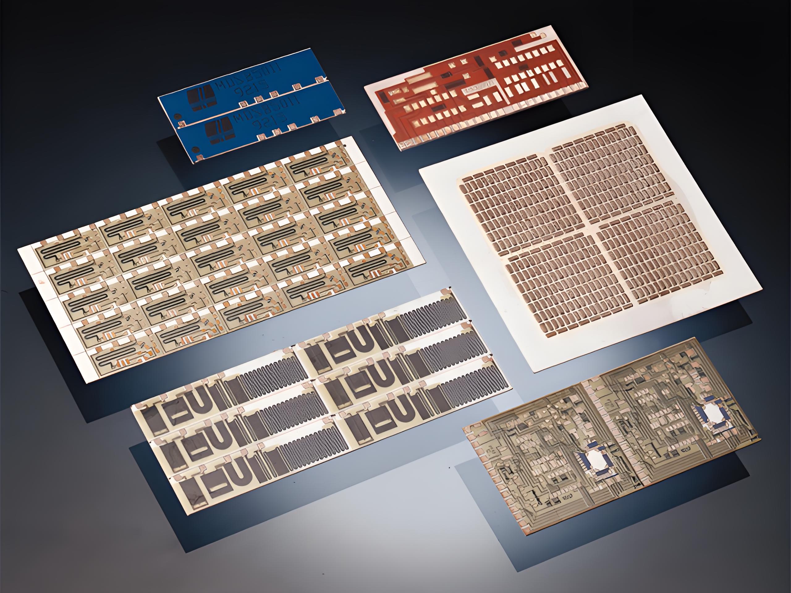
A ceramic PCB, or ceramic circuit board, uses ceramic materials such as aluminum oxide (Al₂O₃), aluminum nitride (AlN), or beryllium oxide (BeO) as its substrate. Unlike traditional FR4 boards, ceramic substrates offer excellent thermal conductivity, high mechanical strength, and superior frequency performance, making them ideal for power electronics, LED lighting, aerospace, and RF applications. Because of their brittleness and hardness, the manufacturing and especially the depanelization process requires special handling and techniques.
Why Need to Depanelize Ceramic Circuit Board?
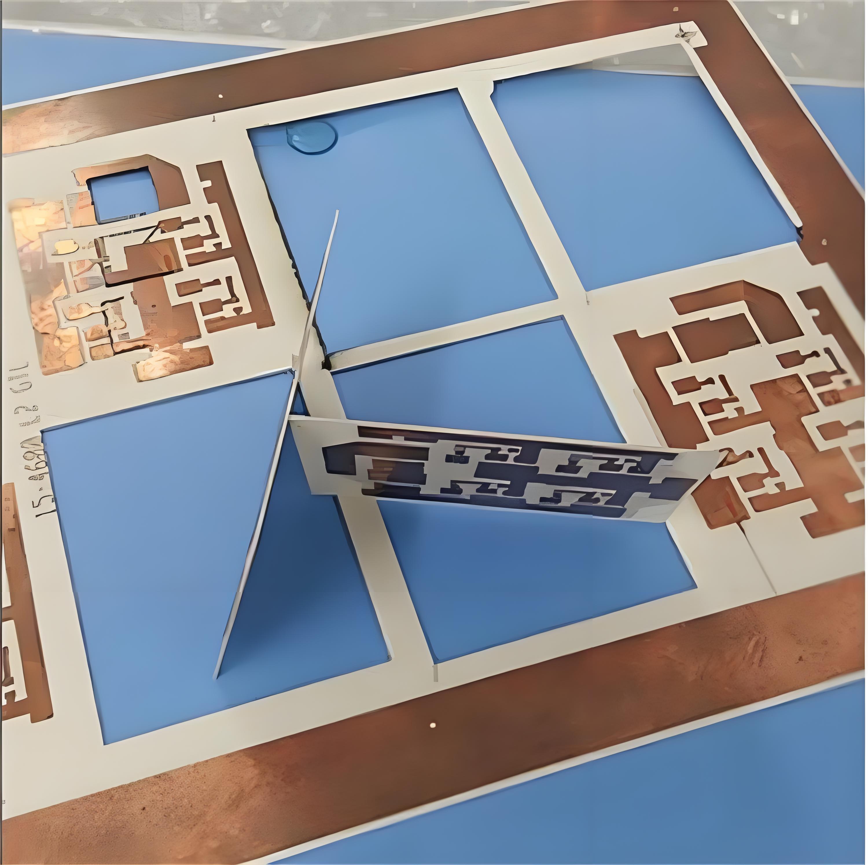
In a production environment, ceramic PCBs are often fabricated in arrays (also known as panels) to streamline processing such as ceramic PCB SMT assembly and reflow soldering. Once all components are mounted and inspection is completed, the individual boards must be separated from the array for packaging and integration into end-user devices. This final separation step is what we refer to as depanelization.
However, depanelizing ceramic PCBs is not as straightforward as FR4 due to the material’s hardness and fragility. Poorly executed cuts can result in cracks, micro-fractures, or edge chipping, compromising both aesthetics and electrical integrity. Therefore, knowing how to de-panel ceramic PCBs properly is essential to maintaining product reliability.
Type of Ceramic PCB Depanelize Methods
Various methods are employed to depanelize ceramic PCBs, each with its own set of pros and cons. Choosing the right method depends on the material type, board thickness, edge quality requirement, production volume, and available equipment.
Diamond Saw Cutting – Precision at a Cost
Diamond saws use high-speed rotating blades embedded with industrial-grade diamonds to cut through ceramic substrates. This method provides excellent dimensional accuracy and minimal burrs. However, it also presents several challenges:
- Tool Wear: Diamond blades wear out over time and require regular replacement.
- Edge Stress: Although cleaner than manual tools, it may still introduce micro-cracks along the edges.
- Setup Time: Not ideal for low-volume or custom designs due to fixture requirements.
For thick and dense ceramic materials like AlN, diamond saws remain a viable choice when ultra-tight tolerances are required.
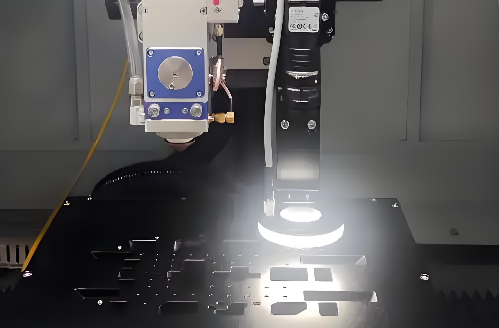
Laser De-paneling – The Preferred Method
Laser de-paneling is considered the most advanced and efficient technique to depanelize ceramic PCBs, especially for high-volume or high-precision applications. It uses a focused laser beam (typically UV or IR wavelengths) to ablate the material along the cutting path.
Advantages include:
- Non-Contact Process: Reduces mechanical stress and eliminates edge chipping.
- High Precision: Enables narrow kerf widths (≤30 µm) and complex cut patterns.
- No Tool Wear: Lasers maintain consistent quality without blade degradation.
- Cleanroom Compatibility: Ideal for medical and aerospace electronics where cleanliness is essential.
One key limitation is the initial capital investment. However, when considering yield, edge integrity, and throughput, laser systems provide superior ROI over time.
Scribe and Break – Traditional but Risky
The scribe and break method involves scoring the ceramic along a predefined line and then applying mechanical force to snap the board apart. This technique is simple and cost-effective for basic layouts but is typically not recommended for high-reliability applications due to:
- Unpredictable Breaks: Inconsistent break lines may damage circuit traces.
- Micro-fractures: Stress propagation can lead to invisible cracks that later cause field failures.
- Limited Material Suitability: Best suited only for thin Al₂O₃ boards (<0.5 mm).
Despite its downsides, some low-cost manufacturing operations still use this method for small-batch production.
What Should I Consider When De-panel a Ceramic PCB?
When determining how to de-panel ceramic PCBs, several factors must be evaluated to minimize risk and ensure consistent quality:
- Material Type: Al₂O₃ is more brittle than AlN but less costly. Choose methods accordingly.
- Board Thickness: Thicker boards may resist scribing and require sawing or laser cutting.
- Trace Proximity: Ensure copper traces are set back from cut lines to prevent damage.
- Production Volume: Higher volumes justify automation (e.g., laser), while prototypes may tolerate manual cutting.
An experienced ceramic PCB manufacturer will always review these parameters during DFM (Design for Manufacturability) discussions to choose the optimal de-paneling approach.
Tips When Manually De-panel Ceramic Board?
If you need to manually depanel ceramic PCBs, especially during prototyping or low-volume runs, here are some key precautions:
- Use Proper Tools: Use a diamond-tipped cutter or fine-grit saw; never standard tools.
- Secure the Board: Clamp the board firmly to prevent vibrations during cutting.
- Cut in Stages: For thick substrates, avoid deep single-pass cuts—use multiple shallow passes instead.
- Wear PPE: Ceramic dust can be harmful. Always wear gloves and a mask.
- Avoid Excess Pressure: Let the tool do the work; excessive force can cause fractures.
Although manual depaneling is not ideal for production use, careful handling can still yield acceptable results if done by skilled technicians.
How to Design Ceramic PCBs for Easier De-paneling?
Optimizing your board design is just as critical as choosing the right cutting method. When working with a ceramic PCB manufacturer, consider these DFM tips:
- Add V-Grooves or Pre-Scored Lines: Helps guide cuts and reduces mechanical stress.
- Keep Components Away from Edges: Leave at least 1 mm clearance to avoid damage during separation.
- Use Rounded Corners in Cutouts: Sharp inside corners can create stress risers and increase fracture risk.
- Incorporate Fiducials and Tooling Holes: These help align cutting paths for automated depaneling systems.
Designing with de-paneling in mind will reduce scrap, improve assembly throughput, and ensure longer lifespan for the end product.
One-Stop Ceramic PCB Manufacturer – Best Technology
When it comes to ceramic circuit boards, Best Technology is your trusted ceramic PCB manufacturer. We specialize in aluminum oxide, aluminum nitride, and BeO ceramic PCBs and offer a full suite of services—from layout review and material selection to precision laser de-paneling.
Our strengths include:
- Advanced Laser Depaneling Machines for crack-free, burr-free cuts
- ISO-certifications ensuring traceability and quality
- Professional Engineering Team to guide your design for manufacturability
- Competitive Pricing even for high-mix, low-volume runs
Whether you're building power modules, RF antennas, or high-temperature LED circuits, we deliver consistent quality and fast turnaround. If you're unsure how to de-panel ceramic PCBs, let our experts assist you with the best methods suited to your application.
FAQs
1. What is the safest method to depanelize ceramic PCBs?
Laser de-paneling is the safest and most precise method due to its non-contact nature.
2. Can I depanel ceramic PCBs using a manual tool?
Yes, but it's risky and suitable only for prototypes. Precision tools and care are essential.
3. Which ceramic material is easiest to depanel?
Al₂O₃ is the most commonly used and easier to process compared to AlN or BeO.
4. What happens if a ceramic board cracks during depaneling?
Even small cracks can lead to complete board failure during operation or thermal cycling.
5. Does Best Technology support custom panel layouts?
Absolutely. We help customers design panel formats that suit both assembly and depaneling needs.
 Products
 About us
 Contact us


