


 HOME
HOME

-

Silicon Nitride Substrate, Silicon Nitride Ceramic Substrate Formula
2025 05,08 -
How to choose the appropriate substrate for ceramic circuit boards?
2023 11,16 -
Laser Cutting or Water Saw Cutting? How To Choose the Best Cutting Solution for Ceramic Circuit Boards
2023 11,13 -
Why Ceramic PCB Is So Expensive?
2023 11,10 -
Which Process Ceramic Circuit Board Is A Better Solution For Semiconductor Refrigerator Chips?
2023 11,06 -
Silicon Printing Circuit Boards For Advancing Electronics
2023 10,27 -
What is the Difference Between HTCC and LTCC Ceramic PCB
2023 10,06 -
What is the Difference Between 96% and 99% Aluminum Oxide in Ceramic PCBs?
2023 09,20 -
Why thick film ceramic PCB is good for oil level sensor in automotive industry?
2023 08,25 -
Statistical analysis of ceramic PCB application fields
2023 08,16 -
Notice of anti-static requirements for PCBA processing and production
2023 08,16 -
Silver Paste: The Best Conductor Material for Via Holes in Thick Film Ceramic Boards
2023 08,16 -
Testing Circuit Board Ceramic Diode Fuses: A Complete Guide
2023 08,07 -
Why DBC is replaced by DPC in ceramic PCB manufacturing?
2023 08,01 -
What is thick film ceramic PCB?
2023 08,02
How to Make Alumina PCB? | Ceramic PCB Acknowledge
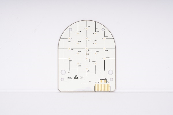
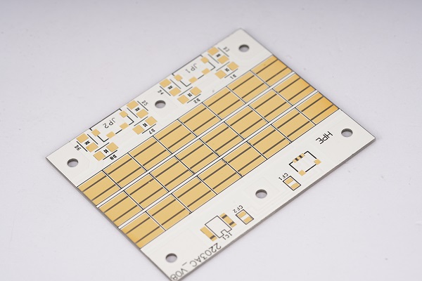
What Is Alumina PCB?
Alumina PCB is a type of ceramic circuit board made using alumina material, also known as aluminum oxide (Al₂O₃). It's not just another PCB. It's stronger, more stable, and perfect for handling high temperatures and power. Unlike FR4 boards, alumina PCBs don’t burn out easily. They also provide great insulation and heat dissipation.
Types of Alumina PCB Materials
The main difference in alumina PCBs comes from the purity of the alumina material. Common types include 96%, 99%, and 99.6% alumina. The higher the purity, the better the electrical insulation and thermal properties.
- 96% alumina: Cost-effective, used in standard applications.
- 99% alumina: Better thermal performance.
- 99.6% alumina: Top-tier, used for sensitive or advanced devices.
The higher the purity, the better the thermal and electrical properties—but also the higher the cost. So, it’s always about balancing need and budget. Each type suits different needs, depending on your budget and performance.
How Thick Is Alumina PCB?
The thickness of alumina PCBs depends on both the substrate and copper layers. Typically, the alumina substrate ranges from 0.25 mm to 1.5 mm, and copper can vary from 17µm (1/2oz) to 210µm (6oz).
If you're building a high-power device, thicker copper might be needed. But for signal transmission or sensor applications, a thin and light board is often enough. Choosing the right thickness helps ensure performance without overspending.
Why Is Alumina So Hard?
Alumina is naturally hard because of its strong ionic bonds between aluminum and oxygen atoms. It’s even used as a substitute for diamonds in cutting tools. This hardness is great for stability, but it also makes machining more difficult. That’s why advanced equipment, like laser drills and diamond saws, are used during production.
Its toughness means it resists wear, scratching, and cracking. This is one reason why alumina PCBs last longer than traditional ones.
How Do You Convert Aluminium to Alumina?
This happens through a process called the Bayer Process. First, bauxite (the raw ore) is crushed and treated with sodium hydroxide. This separates aluminum hydroxide from impurities. Then, the hydroxide is heated in a kiln to produce alumina powder.
Although the process sounds industrial, the result is a fine, white ceramic material ready for use in PCBs. Once converted, alumina becomes a stable, non-conductive, and heat-resistant material—perfect for electronic substrates.
How to Make Alumina Ceramic PCB Board? – Step by Step
Manufacturing an alumina PCB board takes precision and patience. Unlike FR4, you’re working with ceramic, which behaves very differently. Here’s a more detailed look into each step:
1. Substrate Preparation
The process begins with selecting the right alumina substrate—usually 96%, 99%, or 99.6% alumina depending on the heat resistance, insulation, and mechanical properties you need. The raw substrate is then cleaned with ultrasonic waves or plasma to remove dust, oil, and any oxide layers. This cleaning is essential. Even microscopic particles can reduce bonding strength later.
2. Copper Bonding / Deposition
Now comes the metal layer. This can be done using one of the following methods:
- DBC (Direct Bonded Copper): High-purity copper foil is bonded to the alumina under high temperature and pressure in a nitrogen-rich environment.
- DPC (Direct Plated Copper): Copper is sputtered and plated directly onto the substrate. It’s suitable for fine lines and high-density circuits.
- Thick Film Printing: Conductive pastes are screen-printed and fired onto the ceramic surface. This is simpler but less precise.
Each method has different costs and use cases, so this choice must align with your design goals.
3. Circuit Patterning
Once copper is in place, the circuit layout is printed using photolithography. A dry film photoresist is applied, exposed under UV light through a mask, then developed to reveal the circuit. After that, etching removes unwanted copper, leaving only the desired trace pattern.
4. Hole Drilling & Metallization
If your design needs vias or through-holes, they’re made using a laser or mechanical drill. For DPC or DBC, laser drilling is preferred due to alumina's hardness. Once drilled, the holes are cleaned and metalized (plated with copper) to connect top and bottom layers.
5. Surface Finish Application
Finishing protects copper from oxidation and ensures solderability. Common finishes include ENIG (Electroless Nickel Immersion Gold), silver, or OSP. Choosing the right finish depends on your assembly method and shelf-life requirements.
6. Mechanical Cutting / Routing
Once the circuit is done, panels are cut using diamond routers or laser cutters. This process requires exact control to avoid edge chipping and maintain the shape.
7. Final Inspection & Electrical Testing
Each board is tested for continuity, impedance, and alignment. AOI (Automated Optical Inspection) and sometimes X-ray are used to detect internal flaws, especially in multilayer boards. Only perfect boards move forward.
Key Points During Alumina PCB Manufacturing
- Precision: Fine lines and spaces require high alignment accuracy.
- Handling: Alumina is brittle. It must be handled carefully during drilling and cutting.
- Clean Room: Contamination affects adhesion. A clean environment is a must.
- Thermal Management: Heat treatment during copper bonding needs strict control.
Factors That Affect the Price of Alumina PCB
Alumina PCBs tend to cost more than FR4, but there are good reasons for that. Understanding what drives the price can help you plan smarter and reduce unnecessary costs.
1. Alumina Purity Level
Higher purity means better electrical insulation and thermal performance. But it also means a more expensive raw material. If your project doesn’t need ultra-high specs, 96% alumina is often enough and more budget-friendly.
2. Copper Bonding Method
DPC and DBC both offer excellent performance, but their processes differ. DPC requires vacuum deposition and cleanroom plating, which costs more. DBC uses pressure bonding and is more economical for thick copper applications.
3. Circuit Complexity
Designs with fine traces, tight clearances, and small vias take more time to produce. They also require more precise imaging and etching, which can increase scrap rate and overall cost.
4. Number of Layers
Single-layer alumina PCBs are simpler and cheaper to make. Adding a second or third layer requires more copper deposition, alignment steps, and drilling, all of which drive up the price.
5. Copper Thickness
Thicker copper means more material, but also longer etching and bonding times. If you only need signal transmission, thinner copper (like 35µm) is sufficient and cost-effective.
6. Production Volume
Ordering 1–5 pieces costs more per unit due to setup, calibration, and tooling. Once you reach a certain batch size, prices drop significantly. Mass production always brings economies of scale.
7. Lead Time Requirements
Need it fast? That usually means overtime, shift changes, and priority runs—leading to higher pricing. Planning ahead saves money and stress.
8. Special Requirements
Do you need custom cutting, high-frequency support, or special finishes? Each of these adds a bit to the total price, especially if the process isn't standard in the factory.
Tips for Customers to Reduce Cost and Speed Up Delivery
Stick with standard thickness and purity if your project doesn’t need extremes.
- Use single-layer designs when possible.
- Provide clear, error-free Gerber files.
- Plan ahead to avoid rush orders.
- Ask your supplier for advice on cost-saving design tweaks.
A good supplier like Best Technology will guide you on how to get the best value.
Alumina PCB vs. Traditional FR4 PCB
|
Feature |
Alumina PCB |
FR4 PCB |
|
Thermal Conductivity |
20–30 W/m·K |
0.3–0.5 W/m·K |
|
Operating Temperature |
Up to 350°C |
Below 130°C |
|
Mechanical Strength |
Very high |
Moderate |
|
Moisture Resistance |
Excellent |
Fair |
|
Cost |
Higher |
Lower |
|
Best Use Cases |
LED, lasers, RF, power modules |
Consumer electronics, general use |
While FR4 is still widely used, alumina ceramic PCBs are clearly better for demanding applications. They last longer, perform better under stress, and support higher heat.
Your Best Alumina PCB Partner – Best Technology
When you're working with high-performance devices, you need a PCB partner who knows what they’re doing. Best Technology specializes in alumina PCB manufacturing with DPC, DBC, and thick-film ceramic PCB capabilities.
We hold ISO9001, IATF16949, and AS9100 certifications. Our MES system ensures full traceability of every board, and our engineers are available to help with every step—design, prototyping, and volume production.
Whether you’re developing a new LED module or a high-frequency RF application, we’re here to support you with fast quotes, professional service, and consistent quality.
 Products
 About us
 Contact us


