


 HOME
HOME

-

Silicon Nitride Substrate, Silicon Nitride Ceramic Substrate Formula
2025 05,08 -
How to choose the appropriate substrate for ceramic circuit boards?
2023 11,16 -
Laser Cutting or Water Saw Cutting? How To Choose the Best Cutting Solution for Ceramic Circuit Boards
2023 11,13 -
Why Ceramic PCB Is So Expensive?
2023 11,10 -
Which Process Ceramic Circuit Board Is A Better Solution For Semiconductor Refrigerator Chips?
2023 11,06 -
Silicon Printing Circuit Boards For Advancing Electronics
2023 10,27 -
What is the Difference Between HTCC and LTCC Ceramic PCB
2023 10,06 -
What is the Difference Between 96% and 99% Aluminum Oxide in Ceramic PCBs?
2023 09,20 -
Why thick film ceramic PCB is good for oil level sensor in automotive industry?
2023 08,25 -
Statistical analysis of ceramic PCB application fields
2023 08,16 -
Notice of anti-static requirements for PCBA processing and production
2023 08,16 -
Silver Paste: The Best Conductor Material for Via Holes in Thick Film Ceramic Boards
2023 08,16 -
Testing Circuit Board Ceramic Diode Fuses: A Complete Guide
2023 08,07 -
Why DBC is replaced by DPC in ceramic PCB manufacturing?
2023 08,01 -
What is thick film ceramic PCB?
2023 08,02
Introduction to DBC direct bonded copper substrate
Direct bonded copper (DBC) substrates are critical components in high-power electronic systems. Designed to combine excellent thermal conductivity with high electrical insulation, DBC substrates are widely used in industries such as automotive, industrial automation, renewable energy, and aerospace. A direct bonded copper substrate features a thick layer of pure copper bonded directly to a ceramic base—typically aluminum oxide (Al₂O₃) or aluminum nitride (AlN)—through a high-temperature diffusion process.
Unlike traditional PCB technologies that rely on FR-4 or polyimide bases, DBC technology provides superior heat dissipation and thermal stability. So, DBC ceramic PCB is preferred solution in applications where components must operate reliably under extreme heat and electrical loads.
What Are Direct Bonded Copper Substrates?
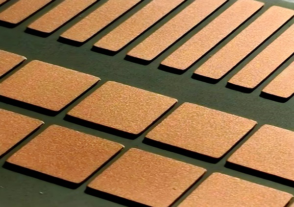
A direct bonded copper substrate is a type of ceramic PCB where a thick layer of copper (around 75um-300um) is bonded directly onto a ceramic base using an oxide-based bonding process. Unlike conventional PCBs that use adhesives, DBC uses high-temperature diffusion bonding to create a strong and thermally conductive joint between copper and ceramic.
This results in exceptional electrical insulation, excellent thermal performance, and robust mechanical support, especially in environments where thermal shock or high voltage is present.
Typical Structure:
- Top Layer: 0.3–0.8 mm Copper
- Middle Layer: Al₂O₃ (Alumina) or AlN (Aluminum Nitride) Ceramic
- Bottom Layer (Optional): Copper for double-sided DBCs
Direct Bonded Copper Ceramic PCB Properties
Direct bonded copper ceramic PCBs are engineered to meet the high demands of power electronics. Here are the key properties that make DBC stand out:
- The copper layer has strong adhesion and corrosion resistance
- Excellent mechanical strength and stable dimensions
- Excellent thermal cycling performance with high reliability
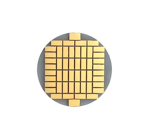
- It can be etched into various graphic structures like a PCB board, without pollution or harm
- It can adapt to temperatures ranging from -55 to 850 degrees Celsius
- Thermal expansion coefficient close to that of silicon and small thermal stress
What Is the Difference Between DBC and AMB Substrates?
Though both DBC (Direct Bonded Copper) and AMB (Active Metal Brazing) technologies serve high-power applications, their bonding methods, cost, and materials differ significantly:
|
Item |
DBC Substrate |
AMB Substrate |
|
Bonding Method |
Copper oxide bonding at high temperatures |
Brazing using active metals (e.g., Ti, Zr) |
|
Ceramic Compatibility |
Al₂O₃, AlN |
AlN, Si₃N₄, BeO |
|
Copper Thickness |
0.3–0.8 mm |
0.3–1.0 mm |
|
Bond Strength |
Moderate to high |
Very high |
|
Cost |
Lower |
Higher |
|
Applications |
Power modules, automotive inverters |
Aerospace, defense, advanced power systems |
Direct bonded copper substrates offer an optimal balance of cost, reliability, and performance, especially for industrial and automotive applications. AMB substrates, while stronger, are reserved for mission-critical systems with extreme demands.
What Is the Thickness of DBC Copper?
The copper thickness in a direct bonded copper substrate typically ranges from:
- 0.3 mm (300 μm) — standard applications
- 0.5 mm (500 μm) — mid-range power modules
- 0.8 mm (800 μm) — high-current, high-power applications
Choosing the right thickness is crucial:
- Thicker copper improves current-carrying capacity and heat dissipation.
- However, it also complicates etching and increases material stress.
- Designers must balance these factors to optimize performance and manufacturability.
What Temperature Is Direct Copper Bonding?
The direct copper bonding process operates between 1065°C and 1083°C, just under the melting point of copper. The process includes:
- Pre-oxidation of Copper Foil: Forms a thin oxide layer on the copper surface.
- Stacking and Lamination: Oxidized copper foil is placed on the ceramic layer.
- High-Temperature Bonding: The assembly is heated in a nitrogen or hydrogen atmosphere, causing the copper to chemically bond with the ceramic.
- Cooling: Ensures the formation of a strong, void-free interface.
This high-temperature process creates a metallurgical bond that can withstand thermal cycling and mechanical stress.
Manufacturing Process of Direct Bonded Copper Ceramic PCB
Direct Bonded Copper ceramic PCB manufacturing process involving ceramic-copper bonding process and the pattern etching on the copper process. Two of them are very important steps during the whole process.
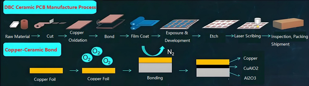
1. Raw Material Preparation
High-purity copper foil and ceramic substrates (Al₂O₃ or AlN) are selected based on the application’s thermal and electrical requirements.
2. Cutting
The copper foil and ceramic substrates are cut to the required size according to the product specifications to ensure proper alignment and minimal material waste.
3. Copper Foil Oxidation
The copper surface undergoes a controlled oxidation treatment to form a uniform Cu₂O (cuprous oxide) layer. This oxide layer is critical for achieving a chemical bond during the high-temperature sintering process.
4. Bonding
The oxidized copper foil is placed on the ceramic substrate and prepared for the direct bonding process.
5. Lamination (Film Coating)
A dry or wet film is applied to the copper surface to serve as a mask for the photolithography process.
6. Exposure & Development
Circuit patterns are transferred to the film using UV exposure. Unexposed areas are then removed using a developing solution to reveal the copper areas to be etched.
7. Etching
The developed board is submerged in a chemical etching solution to remove unwanted copper, leaving behind the desired circuit patterns.
8. Laser Scribing / Cutting
Precision laser scribing or cutting is performed to divide the panels into individual units and prepare them for final inspection and shipment.
9. Inspection, Packaging & Shipment
Each board undergoes a full inspection including appearance, dimensional accuracy, electrical testing, and thermal performance before final packaging and delivery.
Direct Bonded Copper PCB Uses
Direct bonded copper PCBs are used in applications where heat management and electrical insulation are essential:
- Power modules (IGBT, MOSFET)
- LED lighting systems
- Automotive electronics
- Renewable energy systems
- Semiconductor cooler
- Electronic heater
- Power control circuit
- High-frequency switching power supply
- Solid-state relay, automotive electronics
- Solar panel module,
- Receiving system
- Laser machine
Conclusion
Direct bonded copper substrates represent the future of thermal and electrical management in high-performance electronics. Their robust structure, excellent heat dissipation, and high electrical insulation make them a must-have for any power-intensive application.
If you are looking for a manufacturer with extensive experience in direct bonded copper PCB production, Best Technology is your trusted partner. Our ceramic PCBs are manufactured using precise process control, strict quality inspections, and materials sourced from top-tier suppliers. Whether you need prototyping or large-scale production, we offer expert guidance, competitive pricing, and guaranteed reliability.
 Products
 About us
 Contact us


