


 HOME
HOME

-

Silicon Nitride Substrate, Silicon Nitride Ceramic Substrate Formula
2025 05,08 -
How to choose the appropriate substrate for ceramic circuit boards?
2023 11,16 -
Laser Cutting or Water Saw Cutting? How To Choose the Best Cutting Solution for Ceramic Circuit Boards
2023 11,13 -
Why Ceramic PCB Is So Expensive?
2023 11,10 -
Which Process Ceramic Circuit Board Is A Better Solution For Semiconductor Refrigerator Chips?
2023 11,06 -
Silicon Printing Circuit Boards For Advancing Electronics
2023 10,27 -
What is the Difference Between HTCC and LTCC Ceramic PCB
2023 10,06 -
What is the Difference Between 96% and 99% Aluminum Oxide in Ceramic PCBs?
2023 09,20 -
Why thick film ceramic PCB is good for oil level sensor in automotive industry?
2023 08,25 -
Statistical analysis of ceramic PCB application fields
2023 08,16 -
Notice of anti-static requirements for PCBA processing and production
2023 08,16 -
Silver Paste: The Best Conductor Material for Via Holes in Thick Film Ceramic Boards
2023 08,16 -
Testing Circuit Board Ceramic Diode Fuses: A Complete Guide
2023 08,07 -
Why DBC is replaced by DPC in ceramic PCB manufacturing?
2023 08,01 -
What is thick film ceramic PCB?
2023 08,02
2 Layer Alumina substrate PCB | Aluminum Oxide PCB Manufacturer
Are you searching for a reliable solution for heat-resistant and electrically stable PCBs? A 2 layer alumina substrate PCB may be exactly what you need. At Best Technology, we specialize in aluminum oxide PCB manufacturing, providing customers with durable ceramic PCBs designed for high-performance and high-temperature environments. In this guide, we’ll explore the structure, benefits, applications, and production process of these advanced PCBs, and show how we can support your project from start to finish.
What Is 2 Layer Alumina Substrate PCB?
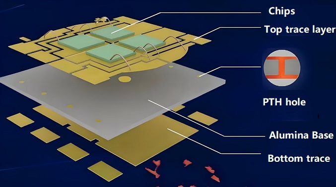
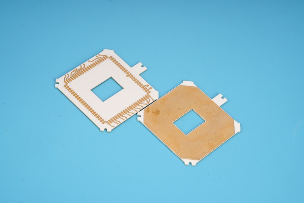
A 2 layer alumina substrate PCB is a type of ceramic printed circuit board that uses aluminum oxide (Al₂O₃) as the core substrate material. It consists of two layers of copper circuitry — one on each side of the ceramic — which are used for signal routing, power distribution, and thermal management.
The use of alumina substrate allows the board to operate efficiently in environments with high temperatures, strong mechanical stress, or high-frequency signals. The two-layer structure offers more routing flexibility and better electrical performance than single-layer ceramic PCBs, especially in compact designs where space is limited.
Why Choose Aluminum Oxide as PCB Substrate?
Aluminum oxide, commonly referred to as alumina, is widely used in the PCB industry for its exceptional thermal and electrical properties. Here are some reasons why it's a top choice for ceramic PCBs:
1. High Thermal Conductivity
Alumina substrates typically have thermal conductivity ranging from 15 W/m·K to 35 W/m·K, helps protect sensitive components from overheating.
2. Excellent Electrical Insulation
Despite its thermal conductivity, alumina also provides strong electrical insulation, with a dielectric strength of up to 20 kV/mm.
3. Mechanical Durability
Alumina is a rigid and stable ceramic material. It resists mechanical wear and thermal shock, making it suitable for applications exposed to vibration, heat, or stress.
4. Cost-Effective Compared to Other Ceramics
While aluminum nitride and silicon carbide offer higher thermal performance, alumina provides an excellent price-to-performance ratio.
5. Compatibility with Various Metallization Methods
Alumina substrates support thick film, DBC (Direct Bonded Copper), DPC (Direct Plated Copper), and other metallization processes, offering flexibility in design and performance.
Applications of 2 Layer Alumina Substrate PCB
Thanks to its thermal, electrical, and mechanical advantages, a 2 layer alumina PCB is used in many demanding applications. Common examples include:
- Power Electronics - Used in DC-DC converters, inverters, and power modules, alumina PCBs handle high currents and voltages while maintaining stable operation.
- LED Lighting Systems - Efficient heat dissipation helps LED modules run cooler and last longer, making these boards ideal for LED drivers, light bars, and displays.
- RF and Microwave Circuits - The dimensional stability and low signal loss of alumina PCBs support high-frequency applications, such as antennas, radar systems, and RF amplifiers.
- Automotive Electronics - Used in engine control units, battery management systems, and sensors, alumina PCBs withstand temperature extremes and vibration found in vehicles.
- Medical Devices - From imaging equipment to implantable electronics, alumina’s biocompatibility and reliability are essential for safe medical applications.
Manufacturing Process of Aluminum Oxide PCBs
Creating a high-quality aluminum oxide PCB requires precise control and specialized equipment. Here’s a simplified overview of our process at Best Technology:
1. Substrate Preparation
We start by selecting alumina sheets of the desired thickness (common options: 0.25mm, 0.5mm, 1.0mm, 1.5mm). These sheets are cleaned to ensure no contaminants affect copper adhesion.
2. Copper Layer Application
Copper can be applied via different methods:
- DBC (Direct Bond Copper): Copper is bonded to the ceramic at high temperatures.
- DPC (Direct Plated Copper): Copper is plated onto the ceramic using chemical deposition.
- Thick Film Printing: Conductive pastes are screen-printed onto the substrate.
Each method offers specific benefits depending on thermal requirements, design complexity, and cost.
3. Circuit Patterning
We use photoresist and etching techniques to form the circuit patterns. This allows precise control over trace width, spacing, and circuit layout.
4. Drilling and Metallization (if needed)
For designs with vias or plated holes, we drill the board and apply conductive materials to form reliable interconnections.
5. Surface Finishing
Finishes such as ENIG (Electroless Nickel Immersion Gold), silver, or OSP are applied for solderability and corrosion protection.
6. Testing and Inspection
Every board is inspected using visual, electrical, and X-ray methods to ensure it meets IPC and customer standards.
2 Layer Alumina PCB vs Traditional FR4 PCB Comparison Chart
|
Item |
2 Layer Alumina PCB |
FR4 PCB |
|
Base Material |
Aluminum Oxide (Al₂O₃, Ceramic) |
FR4 (Glass-reinforced epoxy laminate) |
|
Thermal Conductivity |
15–35 W/m·K |
~0.25–0.3 W/m·K |
|
Maximum Operating Temperature |
250°C – 350°C |
130°C – 140°C (continuous); max ~150°C |
|
Dielectric Strength |
15–20 kV/mm |
~20 kV/mm |
|
Dielectric Constant (Dk) |
9.0–9.8 at 1MHz |
4.2–4.8 at 1MHz |
|
Loss Tangent (Df) |
~0.0001 – 0.0003 |
~0.02 |
|
Thermal Expansion (CTE) |
6–7 ppm/°C (very low, close to silicon) |
~14–18 ppm/°C (higher mismatch with components) |
|
Flexural Strength |
~350 MPa |
~400 MPa |
|
Mechanical Rigidity |
Very high (ceramic, brittle under shock) |
Moderate (more flexible and resilient) |
|
Moisture Absorption |
≤0.01% |
~0.10% |
|
Electrical Insulation |
Excellent even under high temperature |
Good, may degrade under high humidity or heat |
|
Copper Clad Thickness |
Typically 17µm–105µm (½ oz to 3 oz); custom options |
Same range; more variation possible |
|
Board Thickness Range |
0.25mm, 0.5mm, 1.0mm, 1.5mm (standard options) |
0.2mm–3.2mm (widely customizable) |
|
Layer Count |
Typically 1–2 layers; multilayer possible (costly) |
1–30+ layers possible |
|
Manufacturing Cost |
Higher (ceramic material, precise processes) |
Lower (mass production, low-cost material) |
|
Heat Dissipation Capability |
Excellent; suitable for high-power circuits |
Poor; requires heat sinks or thermal vias |
|
RF/Microwave Performance |
Superior (low Df, stable Dk) |
Acceptable for low frequencies |
|
Mechanical Processing |
Requires laser or diamond tools (brittle) |
Standard drilling and routing tools |
|
Environmental Resistance |
High (chemical, moisture, temperature) |
Moderate (susceptible to moisture, delamination) |
|
Common Applications |
Power electronics, LED drivers, RF/microwave, medical |
Consumer electronics, general-purpose circuits |
|
Lifespan |
Longer; stable under harsh conditions |
Shorter in high-heat/high-stress environments |
Alumina PCB Thickness and Tolerance Options
At Best Technology, we offer flexible options to meet your design needs:
- Substrate Thickness: 0.25mm, 0.5mm, 1.0mm, 1.5mm, others on request
- Copper Thickness: 17µm (1/2 oz), 35µm (1 oz), 70µm (2 oz), 105µm (3 oz)
- Tolerances: ±10% or better, based on your requirements
For more specifications about alumina PCB, welcome to view our alumina ceramic PCB capability.
Alumina PCB Price Factors
The cost of alumina PCBs depends on several factors, such as:
- Board size and shape
- Copper weight and substrate thickness
- Layer count (1-layer, 2-layer, multilayer)
- Metallization method (DBC, DPC, thin film, thick film, AMB…)
- Surface finish
- Order quantity
- Special standard followed or testing
At Best Technology, we offer competitive pricing and transparent quotes, whether you need a prototype or mass production.
Why Choose Best Technology as Your Aluminum Oxide PCB Manufacturer?
At Best Technology, we combine professional service, global delivery, and competitive pricing to meet your needs. Here’s how we add value to your project:
- One-stop services from 0 to 1
- No MOQ & Fully Flexible
- 99% Customer Satisfaction with IATF16949 certificated
- Professional ceramic PCB engineering support
- Fast delivery and global shipping options
- Competitive pricing for small and large batches
- Factory based prices and mature manufacturing techniques
- Various metallization options: thick film, DPC, DBC, thin film, etc
How to Get a Quote for 2 Layer Alumina Substrate PCB?
To get started, just provide the following:
- Gerber files or PCB drawings
- Required thicknesses and finishes
- Quantity needed
- Any special instructions or certifications
Contact us via email at sales@bstceramicpcb.com or our online form, and we’ll respond with a detailed, no-obligation quote.
FAQs
1. What’s the max operating temperature of alumina PCB?
Most alumina PCBs can operate up to 350°C, depending on design and materials.
2. Do you support multilayer ceramic PCBs?
Yes, we offer multilayer ceramic PCB options based on your design needs. We can make HTCC and LTCC ceramic PCB as well.
3. Are your PCBs RoHS compliant?
Yes, all materials comply with RoHS and REACH regulations.
4. What is the lead time for prototypes?
It depends on the design complexity of the ceramic PCB. For simple ceramic PCB, 7-10 working days is okay.
5. Can you offer design assistance?
Yes, we provide free DFM checks and engineering support.
 Products
 About us
 Contact us


