


 HOME
HOME

-

Silicon Nitride Substrate, Silicon Nitride Ceramic Substrate Formula
2025 05,08 -
How to choose the appropriate substrate for ceramic circuit boards?
2023 11,16 -
Laser Cutting or Water Saw Cutting? How To Choose the Best Cutting Solution for Ceramic Circuit Boards
2023 11,13 -
Why Ceramic PCB Is So Expensive?
2023 11,10 -
Which Process Ceramic Circuit Board Is A Better Solution For Semiconductor Refrigerator Chips?
2023 11,06 -
Silicon Printing Circuit Boards For Advancing Electronics
2023 10,27 -
What is the Difference Between HTCC and LTCC Ceramic PCB
2023 10,06 -
What is the Difference Between 96% and 99% Aluminum Oxide in Ceramic PCBs?
2023 09,20 -
Why thick film ceramic PCB is good for oil level sensor in automotive industry?
2023 08,25 -
Statistical analysis of ceramic PCB application fields
2023 08,16 -
Notice of anti-static requirements for PCBA processing and production
2023 08,16 -
Silver Paste: The Best Conductor Material for Via Holes in Thick Film Ceramic Boards
2023 08,16 -
Testing Circuit Board Ceramic Diode Fuses: A Complete Guide
2023 08,07 -
Why DBC is replaced by DPC in ceramic PCB manufacturing?
2023 08,01 -
What is thick film ceramic PCB?
2023 08,02
Alumina Circuit Board: Types, Features & Applications
What is an Alumina Circuit Board?
An alumina circuit board is a ceramic-based PCB made from aluminum oxide (Al₂O₃), a material known for its excellent thermal conductivity, electrical insulation, and mechanical strength. Unlike traditional PCBs that use FR4 (glass-reinforced epoxy) or metal core bases, alumina ceramic PCBs offer better performance in high-temperature and high-power environments. The dense ceramic substrate not only resists heat and corrosion but also minimizes dielectric loss and supports precise signal transmission.
These boards are commonly used in sectors such as aerospace, medical electronics, industrial automation, automotive systems, and LED lighting, where performance, longevity, and reliability are non-negotiable. Due to the exceptional thermal dissipation of alumina, these PCBs help protect sensitive components from overheating, ultimately improving the efficiency and lifespan of electronic devices.
Types of Alumina PCB
Alumina PCBs come in various purity grades. Each grade has its own thermal, mechanical, and electrical performance characteristics. Choosing the right type depends on the application’s temperature demands, dielectric requirements, and budget.
1. 96% Alumina PCB
The 96% alumina PCB is the most common type used in the electronics industry. It offers a great balance between cost and performance. With a thermal conductivity of around 18–22 W/m·K, it performs significantly better than standard FR4 PCBs. It has moderate dielectric strength, making it suitable for many commercial and industrial applications. It’s widely used in LED circuits, power electronics, and sensor modules, where moderate thermal performance is needed at a competitive price.
2. 99% Alumina PCB
The 99% alumina PCB provides higher thermal conductivity (around 25 W/m·K) and greater dielectric strength. This makes it ideal for more sensitive or high-frequency applications where lower electrical losses are required. These are used in RF modules, microwave circuits, and higher-end power control devices. This grade offers better chemical resistance and can perform well in harsh environments.
3. 99.6% Alumina PCB
The 99.6% alumina PCB is the highest purity ceramic board typically used in electronic manufacturing. With thermal conductivity reaching up to 30 W/m·K and very low electrical loss, it supports advanced functions in aerospace, defense, medical implants, and semiconductor processing. The high purity improves surface quality and resistance to ionic contamination, ensuring longer operational life and high reliability even in vacuum or extreme conditions.
Features and Characteristics of Alumina Ceramic PCB
- Excellent Thermal Conductivity
- High Electrical Insulation
- Low Thermal Expansion
- Outstanding Chemical and Corrosion Resistance
- Superior Moisture Resistance
- High Mechanical and Compressive Strength
- Wear and Tear Resistance
- Radiation Resistance
- High Operating Temperature Range
- Better Performance at High Frequencies
- Lightweight and Compact Design
- Light Reflectivity
- Dimensional Stability
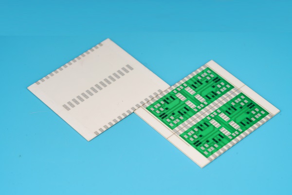
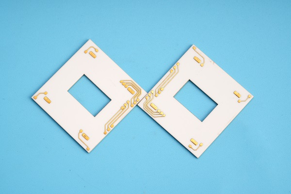
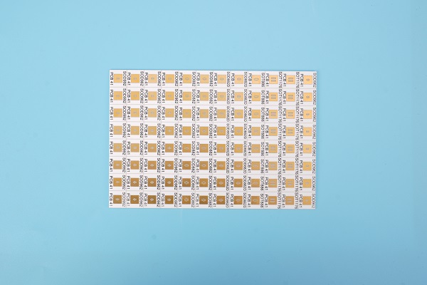
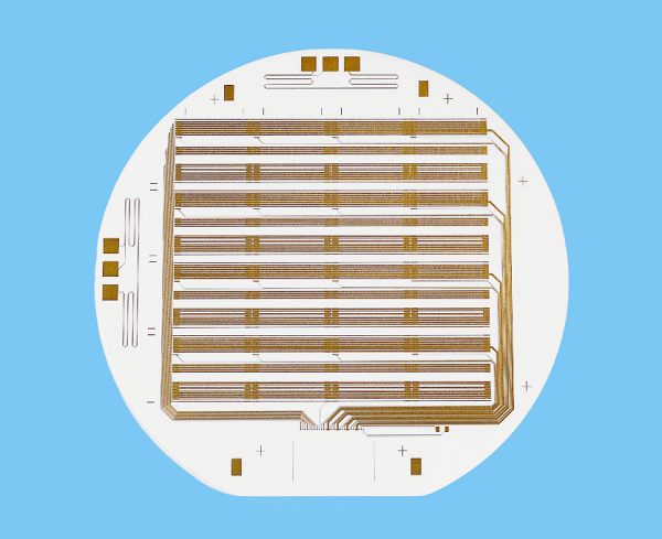
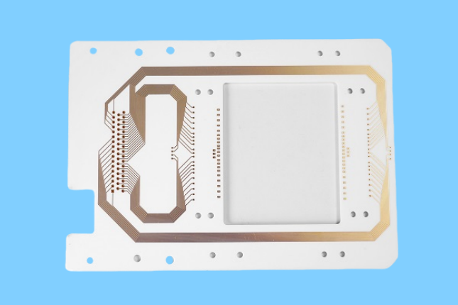
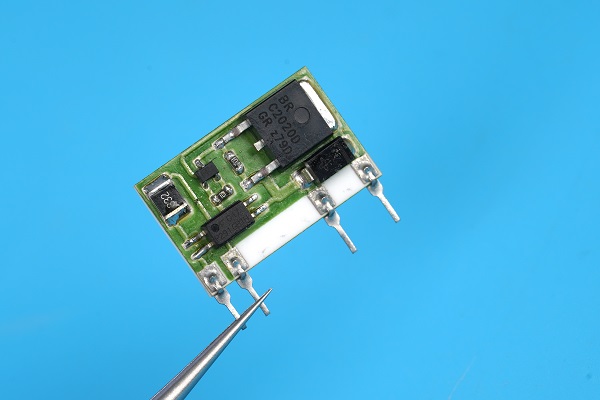
Photos of Alumina Ceramic PCB
Here are some alumina ceramic PCB photos that we made before. They have different shapes, sizes, and uses the different purities (but it can’t be identified from photos.)
Alumina Ceramic PCB for Educations
Alumina Ceramic PCB for Small Chips
Alumina Ceramic PCB for High Power Lighting
Alumina Ceramic PCB for Science Development
Alumina Ceramic PCB with Components
What is the Difference Between Aluminum and Alumina PCB?
While aluminum and alumina PCBs may sound and seems similar, but they differ significantly in composition, structure, and performance. Actually, aluminum PCB is a metal-based PCB, which uses aluminum core as the base, while alumina PCB is a kind of ceramic PCB, while its core is alumina oxide materials.
Unlike aluminum PCBs, alumina boards are non-metallic and provide better heat resistance, chemical durability, and stable performance in extreme environments. Alumina PCBs can handle higher operating temperatures, typically ranging from 350°C up to 1500°C, which aluminum PCBs cannot withstand. Aluminum PCBs are typically used in LED lighting, automotive systems, and power modules, where moderate thermal performance is acceptable.
Due to the aluminum PCB is made by metal base, it has heavier weight than alumina ceramic PCB. Meanwhile, under the same design and requirements, aluminum PCB is much cheaper than that alumina PCB. From a market aspect, aluminum metal PCB is always used in low to middle lighting systems like our home appliance lighting, street lighting, garden lights, but alumina ceramic PCB always used in high-end applications like medical devices, aerospace. Here is a detailed comparison table between aluminum PCB and alumina PCB:
|
Feature |
Aluminum PCB |
Alumina PCB |
|
Material |
Metal core with dielectric layer |
Ceramic (Aluminum Oxide – Al₂O₃) |
|
Electrical Insulation |
Requires insulating layer |
Naturally excellent insulation |
|
Thermal Conductivity |
1–3 W/m·K |
22–24 W/m·K |
|
Operating Temperature |
Up to 150°C |
350°C to 1500°C |
|
Mechanical Strength |
Moderate rigidity |
High compressive and structural strength |
|
Thermal Expansion |
Higher expansion (may stress solder joints) |
Low expansion (6–8 ppm/°C) |
|
Moisture Resistance |
Requires protective coating |
Hermetic, zero water absorption |
|
Chemical Resistance |
Prone to corrosion without treatment |
Excellent resistance to chemicals and corrosion |
|
Cost |
More affordable |
Higher cost due to ceramic processing |
|
Manufacturing Complexity |
Easier and faster to produce |
Requires advanced fabrication methods |
|
Design Complexity |
Best for single or double layers |
Supports high-density, multilayer circuits |
|
Common Applications |
LED lights, power modules, automotive electronics |
Aerospace, RF systems, medical devices, military systems |
|
Durability in Harsh Environments |
Limited |
Superior for extreme conditions |
|
Outgassing |
Moderate |
Very low – suitable for vacuum environments |
Design Considerations of Alumina Circuit Board
Designing an alumina circuit board involves more than just selecting a ceramic substrate. Engineers must account for a range of material-specific behaviors and limitations that impact functionality, manufacturability, and long-term reliability. Here are the most important considerations to keep in mind when working with alumina ceramic PCBs:
1. Material Thickness and Substrate Selection
Alumina ceramic boards come in various thicknesses, typically ranging from 0.25 mm to 2.0 mm. The selection of thickness depends on mechanical strength requirements, thermal management needs, and size constraints. Thinner boards dissipate heat more efficiently and save space but can be fragile under mechanical stress. For heavy-duty or large-format applications, thicker substrates provide better durability and rigidity.
2. Trace Width and Spacing
Alumina substrates are rigid and brittle, so laser or photolithographic processes are used to define trace patterns. Because of the material’s hardness and zero flexibility, minimum trace width and spacing should be larger than those used on FR4 boards. Generally, a minimum of 4 mils (0.1 mm) is recommended for consistent etching and conductivity.
3. Via and Hole Design
Drilling vias or mounting holes in alumina requires precision machining. Laser drilling or ultrasonic techniques are preferred over mechanical methods to avoid cracking. Unlike metal-core PCBs, plated-through holes are more difficult to implement and require specialized metallization processes. Designers should minimize the number of vias and use filled or blind vias if multilayer integration is necessary.
4. Metallization and Conductor Materials
Conductive layers on alumina PCBs are usually made with thick-film or thin-film deposition techniques, using materials such as silver, gold, palladium, tungsten, or molybdenum-manganese. Each metal has trade-offs between adhesion strength, conductivity, and cost. Silver offers great conductivity but is more prone to migration, while tungsten is robust but more difficult to process. Choice of metallization depends on the application’s voltage, frequency, and environmental exposure.
Best Technology is a 19+ years experienced ceramic PCB manufacturer, we have our own ceramic factory in Shenzhen city and Anhui city, China. Half of our engineers have over 10 years experiences in this industry, so we can provide the best solution for you. We can make various metallization process, like thick film ceramic PCB, DPC alumina PCB, DBC ceramic PCB and so on. If you are interested in our ceramic capability, you are welcome to leave your comments or directly contact our engineer sales.
Alumina Ceramic PCB Applications
- Semiconductor devices
- High-power LED Chip
- Wafter Street light
- Wafer chips
- Fuel Sensor
- Electric power transmitter modules
- Solar cell
- Sensor
- Telecom device
- Radar systems
- Navigation systems
- Industrial equipment
- RF & Microwave modules
- High power LED lighting systems
High-Quality Alumina Circuit Board Manufacturer – Best Technology
If you are looking for a reliable alumina circuit board manufacturer, please do not miss out Best Technology! As a leading ceramic manufacturer in China, we have over 18 years experiences and mature techniques that can meet your special requirements. What we provide not only limited to alumina ceramic PCB, but also including aluminum nitride (AlN) ceramic PCB, BeO ceramic PCB, ZrO2 ceramic PCB, Si3N4 ceramic PCB and ceramic packages. We can produce high precision ceramic circuit board using DPC processing, heavy copper traces using DBC processing, silkscreen printing process like thick film technology, AMB active metal brazed technology, HTCC and LTCC co-fired technology.
If choose us, you can enjoy:
- ISO9001, ISO13485 (medical), IATF16949 (automotive), and AS9100D (aerospace) certified quality-controlled product.
- Every alumina circuit board is crafted with rigorous quality checks, from material selection to final testing.
- We use laser cutters, precision CNC machines, and automated screen printers to meet complex specs.
- Whether you need thick-film printing, DPC, or direct copper bonding, our team is skilled in every approach.
- Our sales are engineered sales, they are very professional, can provide respond fast, understand your technical goals, and provide full traceability via our MES system.
- We offer custom ceramic PCB solutions. From prototypes to high-volume orders, we tailor every board to fit your exact electrical, mechanical, and thermal needs.
FAQs
Q1: Why the DCB ceramic PCB surface easy yellow during the production?
We always see the yellow surface in the DCB ceramic PCB surface although it does not affect the function, but looks unbeautiful. In order to strongly combine the copper with ceramic substrate, especially when the copper is little, the exposed more substrate we need to do a special sinters process under appropriate high temperature, so it caused.
it's unavoidable, we need to check and choose the better to ship out.
Q2: Can thick film ceramic PCB with gold paste conductors have through-holes?
No, through-holes must be made with special silver paste, as silver paste and gold paste are incompatible.
Q3: If the AgPd conductor on thick film ceramic PCB oxidizes, how can it be handled?
The surface can be rubbed with an eraser.
Q4: What is the dwell time at peak temperature?
8 minutes to 10 minutes.
Q5: What is the standard thickness for ceramic PCB?
For Ceramic PCB, 0.635mm (0.025”) is the standard and maximum thickness is 0.04” (1.0mm) only! Products
 About us
 Contact us


