


 HOME
HOME

-

Silicon Nitride Substrate, Silicon Nitride Ceramic Substrate Formula
2025 05,08 -
How to choose the appropriate substrate for ceramic circuit boards?
2023 11,16 -
Laser Cutting or Water Saw Cutting? How To Choose the Best Cutting Solution for Ceramic Circuit Boards
2023 11,13 -
Why Ceramic PCB Is So Expensive?
2023 11,10 -
Which Process Ceramic Circuit Board Is A Better Solution For Semiconductor Refrigerator Chips?
2023 11,06 -
Silicon Printing Circuit Boards For Advancing Electronics
2023 10,27 -
What is the Difference Between HTCC and LTCC Ceramic PCB
2023 10,06 -
What is the Difference Between 96% and 99% Aluminum Oxide in Ceramic PCBs?
2023 09,20 -
Why thick film ceramic PCB is good for oil level sensor in automotive industry?
2023 08,25 -
Statistical analysis of ceramic PCB application fields
2023 08,16 -
Notice of anti-static requirements for PCBA processing and production
2023 08,16 -
Silver Paste: The Best Conductor Material for Via Holes in Thick Film Ceramic Boards
2023 08,16 -
Testing Circuit Board Ceramic Diode Fuses: A Complete Guide
2023 08,07 -
Why DBC is replaced by DPC in ceramic PCB manufacturing?
2023 08,01 -
What is thick film ceramic PCB?
2023 08,02
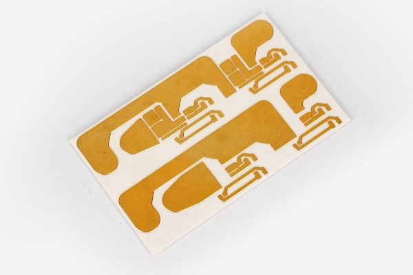
What is Direct Bonded Copper DBC Ceramic PCB?
What is Direct Bonded Copper Ceramic PCB?
A direct bonded copper ceramic PCB, or DBC/DCB ceramic PCB, is a type of ceramic circuit board that coating a thicker layer (commonly 0.3-0.8mm thickness) of copper directly onto a ceramic substrate. This process is achieved through high-temperature oxidation, creating a strong metallurgical bond between the copper and ceramic. Unlike conventional PCBs, there’s no adhesive layer, which means better thermal performance and stronger mechanical stability. DBC boards are commonly used where high voltage and current need to flow through compact circuits, without overheating or failure. These boards are especially critical in sectors that demand exceptional reliability and heat resistance.
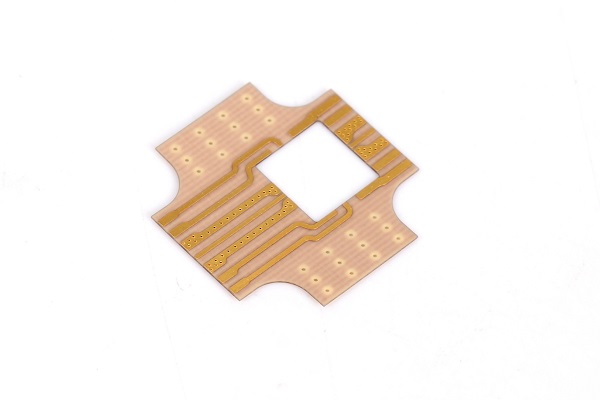
DBC Ceramic PCB Structure
The structure of DBC ceramic circuit board is mainly composed of ceramic substrate, copper foil and metallization layer. Its structural distribution is generally as follows:
- Ceramic substrate: The core of DBC ceramic substrate is ceramic substrate, which is generally distributed as the base support layer at the bottom side, and usually uses aluminum oxide (Al2O3) or aluminum nitride (AlN) as the insulating material. The thermal conductivity of aluminum oxide is 24W/(m·K), while the thermal conductivity of aluminum nitride is as high as 170W/(m·K).
- Copper foil: The second layer is copper foil. Copper foil is eutectic sintered with the ceramic substrate at high temperature to form a tightly bonded composite. Copper foil has good electrical and thermal conductivity, which can effectively reduce the thermal stress between the chip and the substrate.
- Metallization layer: The copper foil is metallized on top layer. The circuit is formed by etching to ensure good electrical conductivity. The design and manufacture of the metallization layer have an important influence on the performance of the substrate.

Advantages of DBC Ceramic PCB
- Exceptional Heat Dissipation: Copper-ceramic interface removes heat efficiently.
- High Current Capacity: Handles dense electrical loads with minimal thermal resistance.
- Long-Term Reliability: No organic materials means less aging and failure risk.
- Mechanical Strength: Resists vibrations, thermal cycles, and environmental stress.
- Compact Design Capability: Ceramic’s insulation allows tighter trace spacing.
- High Voltage Insulation: Safely operates in high-voltage systems without breakdown.
- Chemical Resistance: Performs well in chemically harsh environments.
- CTE that can match with Si
DBC ceramic PCB vs. DPC ceramic PCB
DBC and DPC Ceramic PCBs differ significantly in manufacturing processes, conductor thickness, performance, and application scenarios.
1. Manufacturing Process
- DBC Ceramic PCB:
The Direct Bonded Copper ceramic PCB is manufactured by introducing oxygen at a high temperature (between 1065°C and 1083°C) between the copper and ceramic. This forms a Cu-O eutectic liquid, which then reacts to create an intermediate phase (such as CuAlO₂ or CuAl₂O₄), resulting in a chemical metallurgical bond between the copper and the ceramic substrate. The circuit pattern is then formed on the ceramic base using photolithography techniques.
- DPC Ceramic PCB:
The Direct Plated Copper (DPC) ceramic PCB starts with pre-cleaning the ceramic substrate. A copper seed layer is then sputtered onto the surface using semiconductor processing technology. The circuit pattern is defined through a series of photolithographic steps including exposure, development, etching, and resist stripping. Finally, copper thickness is increased through electroplating or electroless plating to complete the metallization process.
2. Conductor Thickness
- DBC Ceramic PCB:
DBC boards typically feature thicker copper layers, usually ranging from 300µm to 800µm, due to the nature of the manufacturing process.
- DPC Ceramic PCB:
DPC boards have much thinner copper layers, usually between 18µm and 35µm, and generally not exceeding 100µm. If the required copper thickness falls between 100µm and 300µm, DBC is usually recommended instead.
3. Performance Differences
- DBC Ceramic PCB:
Thanks to the thicker copper layer, DBC PCBs offer excellent thermal conductivity, making them suitable for high-power applications.
- DPC Ceramic PCB:
DPC PCBs provide better surface smoothness due to the thinner copper, which is ideal for producing fine-pitch circuits. Additionally, since DPC is manufactured at relatively lower temperatures, it avoids thermal stress on materials or circuit structures.
4. Via Capability
Due to differences in the manufacturing process, DBC ceramic PCBs are typically used for thick copper layers and do not support via (through-hole) design. In contrast, DPC ceramic PCBs can support vias. Titanium plays a bonding role in DPC, and the circuit is formed through magnetron sputtering.
5. Operating Temperature
DPC ceramic PCBs generally have a maximum operating temperature of around 300°C. In contrast, DBC ceramic PCBs are produced under high temperatures and theoretically can operate at temperatures up to 1000°C.
6. Cost
DBC ceramic PCBs are relatively less expensive than DPC. This is due to their more mature manufacturing process, lower material costs, and simpler production. DPC PCBs, on the other hand, require more precise circuit fabrication, leading to higher equipment and process costs.
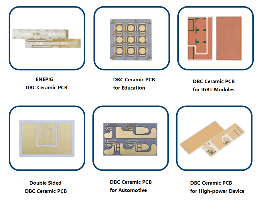
DBC ceramic PCB applications
- Power modules
- IGBTs
- MOSFETs
- EV systems
- Solar inverters
- LED lighting systems
- Medical imaging equipment
- Wind turbines
- Renewable energy
- RF & Telecom
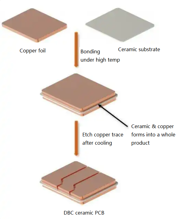
DBC Ceramic PCB Manufacturing Process – Step by Step
The production of DBC ceramics involves several precise and controlled steps to ensure the quality and performance of the final product.
Step 1: Surface Preparation
The ceramic substrate, typically made of materials like aluminum oxide (Al₂O₃) or aluminum nitride (AlN), is thoroughly cleaned. This removes dust, grease, and any surface contaminants to ensure proper bonding with the copper foil.
Step 2: Copper Foil Placement
A high-purity copper sheet is placed directly onto the surface of the ceramic substrate. The copper layer is usually thick—ranging from 300µm to 800µm—suitable for high current handling.
Step 3: Controlled Atmosphere Heating
The assembly is heated in a furnace under a specific oxygen-controlled environment. The temperature rises to between 1065°C and 1083°C, the eutectic point of copper and oxygen.
Step 4: Formation of Eutectic Liquid
At this high temperature, a Cu-O eutectic liquid is generated at the interface between the copper and ceramic. This reactive liquid promotes the formation of a bonding layer between the two materials.
Step 5: Chemical Metallurgical Bonding
The copper chemically reacts with the ceramic substrate, forming intermediate bonding phases such as CuAlO₂ or CuAl₂O₄ (in the case of Al₂O₃ substrates). This reaction creates a strong, stable bond between the copper and ceramic—far stronger than mechanical adhesion.
Step 6: Controlled Cooling
Once the bond has formed, the assembly is slowly cooled down in a controlled manner. This prevents thermal stress, cracking, or delamination of the copper layer from the ceramic.
Step 7: Photolithography for Circuit Patterning
The bonded copper layer is then coated with a photoresist. Using UV light and a mask, the required circuit layout is exposed onto the board.
Step 8: Developing and Etching
The exposed pattern is developed and the unwanted copper is etched away using chemical solutions, leaving only the desired circuit traces.
Step 9: Stripping and Cleaning
After etching, the remaining photoresist is stripped off. The board is cleaned again to remove any residues or contaminants.
Step 10: Surface Finish (Optional)
Depending on the end application, a protective or functional surface finish (such as ENIG, silver, or OSP) can be applied to enhance solderability and oxidation resistance.
Here is a simple manufacturing process flow chart of DBC ceramic PCB:
Challenges and Limitations of DBC ceramic PCB
While highly beneficial, DBC ceramic PCBs do come with a few limitations:
- Application limitations
Although DBC ceramic substrates are widely used in power semiconductor module packaging, coolers, and high-temperature gaskets, their application range is relatively limited. Due to their wider line traces and specific processing requirements, they are not suitable for all application scenarios.
- Compatibility issues with other materials
DBC ceramic substrates may require special treatment or adaptation during integration with other electronic components or systems to ensure good electrical and mechanical connections.
- Environmental adaptability
Although DBC ceramic substrates have excellent heat resistance and chemical stability, their performance may be affected under extreme environmental conditions. For example, long-term use in high temperature environments may cause bubble expansion on the bonding surface, affecting the stability and life of the product.
Why Choose Best Technology as Your DBC Ceramic PCB Supplier?
At Best Technology, we specialize in the design and production of high-reliability ceramic PCBs, including DBC.
Here's why clients choose us:
✅ Certified Quality: ISO-certificated, ISO9001, ISO13485, IATF16949, AS9100D.
✅ Full Traceability: MES system tracks every board from start to finish.
✅ Engineering Support: We help with layout, stack-up, and DFM analysis.
✅ Custom Options: Choose your substrate, copper thickness, and surface finish.
✅ Strict QC: AOI, electrical testing, and thermal reliability checks.
✅ Full Turnkey Service: We offer one-stop service from ceramic PCB design to final assembly, we can even assemble it with flexible PCBs.
✅ Global Shipping: Fast turnaround for samples and production orders.
We don't want to be your one-off supplier—we partner with you to ensure long-term success in your product.
Frequently Asked Questions (FAQs)
Q1: What’s the typical copper thickness used in DBC ceramic PCBs?
Standard options range from 0.3 mm to 0.8 mm, but thicker layers are available for higher current needs.
Q2: Can I use DBC PCBs in outdoor applications?
Yes, especially with AlN substrate. They resist thermal shock, moisture, and UV damage.
Q3: Is DBC better than FR4 for heat management?
Absolutely. Ceramic has far higher thermal conductivity than FR4, and direct copper bonding enhances this benefit.
Q4: Are DBC ceramic PCBs suitable for flexible or wearable electronics?
No. Ceramic is rigid and brittle, not suited for bendable or flexible devices.
Q5: What’s the main advantage of using AlN over Al₂O₃?
Aluminum nitride (AlN) provides higher thermal conductivity, up to 170 W/m·K, making it ideal for high-power or thermally demanding applications.
 Products
 About us
 Contact us


