


 HOME
HOME

-

Silicon Nitride Substrate, Silicon Nitride Ceramic Substrate Formula
2025 05,08 -
How to choose the appropriate substrate for ceramic circuit boards?
2023 11,16 -
Laser Cutting or Water Saw Cutting? How To Choose the Best Cutting Solution for Ceramic Circuit Boards
2023 11,13 -
Why Ceramic PCB Is So Expensive?
2023 11,10 -
Which Process Ceramic Circuit Board Is A Better Solution For Semiconductor Refrigerator Chips?
2023 11,06 -
Silicon Printing Circuit Boards For Advancing Electronics
2023 10,27 -
What is the Difference Between HTCC and LTCC Ceramic PCB
2023 10,06 -
What is the Difference Between 96% and 99% Aluminum Oxide in Ceramic PCBs?
2023 09,20 -
Why thick film ceramic PCB is good for oil level sensor in automotive industry?
2023 08,25 -
Statistical analysis of ceramic PCB application fields
2023 08,16 -
Notice of anti-static requirements for PCBA processing and production
2023 08,16 -
Silver Paste: The Best Conductor Material for Via Holes in Thick Film Ceramic Boards
2023 08,16 -
Testing Circuit Board Ceramic Diode Fuses: A Complete Guide
2023 08,07 -
Why DBC is replaced by DPC in ceramic PCB manufacturing?
2023 08,01 -
What is thick film ceramic PCB?
2023 08,02
Types of Ceramic PCB Metallization Process | BstCeramic PCB
Ceramic circuit boards stand out for their strength, thermal performance, and stability—but what really brings them to life is the metallization process. In simple terms, ceramic metallization is how conductive metals are bonded onto the ceramic surface to form the circuit paths, and the method you choose can make or break your application.
Whether you're powering a high-voltage inverter, designing compact RF modules, or building multilayer microelectronic circuits, selecting the right ceramic PCB metallization process is crucial. Each method offers different advantages in conductivity, durability, thermal performance, and cost.
Let’s explore the most widely used ceramic metallization techniques: Thick Film, Thin Film, DPC, DBC, HTCC, LTCC, and AMB—and see how each one fits different applications.
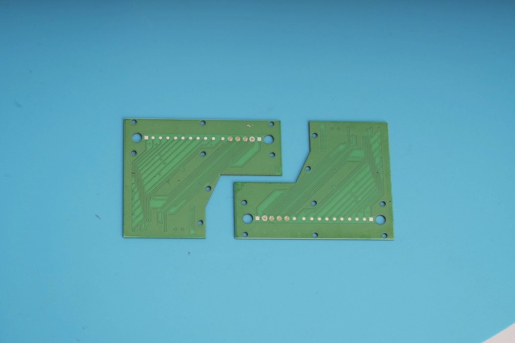
Thick Film Ceramic PCB
Thick film technology is widely used for simple circuit layouts and cost-sensitive applications. In this process, conductive pastes (typically silver or gold) and resistor pastes are screen-printed onto a ceramic substrate—usually alumina. After printing, the board is fired at high temperatures to cure the materials.
Advantages:
- Lower cost for small batches
- Simple process with minimal tooling
- Great for low to moderate-density circuits
Considerations:
- Limited precision for fine lines
- Not ideal for high-density or multilayer boards
- Conductive pastes can be prone to electromigration under high humidity
This method is popular for automotive sensors, heater circuits, and LED packages where simplicity and cost efficiency matter.
Thin Film Ceramic PCB
Thin film PCBs are used in high-end, miniaturized applications. This process involves depositing a very thin metal layer (often gold, platinum, or titanium) onto the ceramic using vacuum deposition or sputtering. Photolithography and etching define extremely fine circuit features.
Advantages:
- Ultra-fine resolution for microelectronics
- Excellent stability and precision
- Great for RF modules, filters, and high-frequency circuits
Considerations:
- Higher cost due to sophisticated equipment
- Limited metal thickness and current-carrying capability
- Better suited for low-power, precision applications
You’ll often find thin film PCBs in RF front ends, optical devices, and military-grade components.
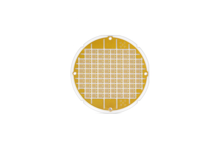
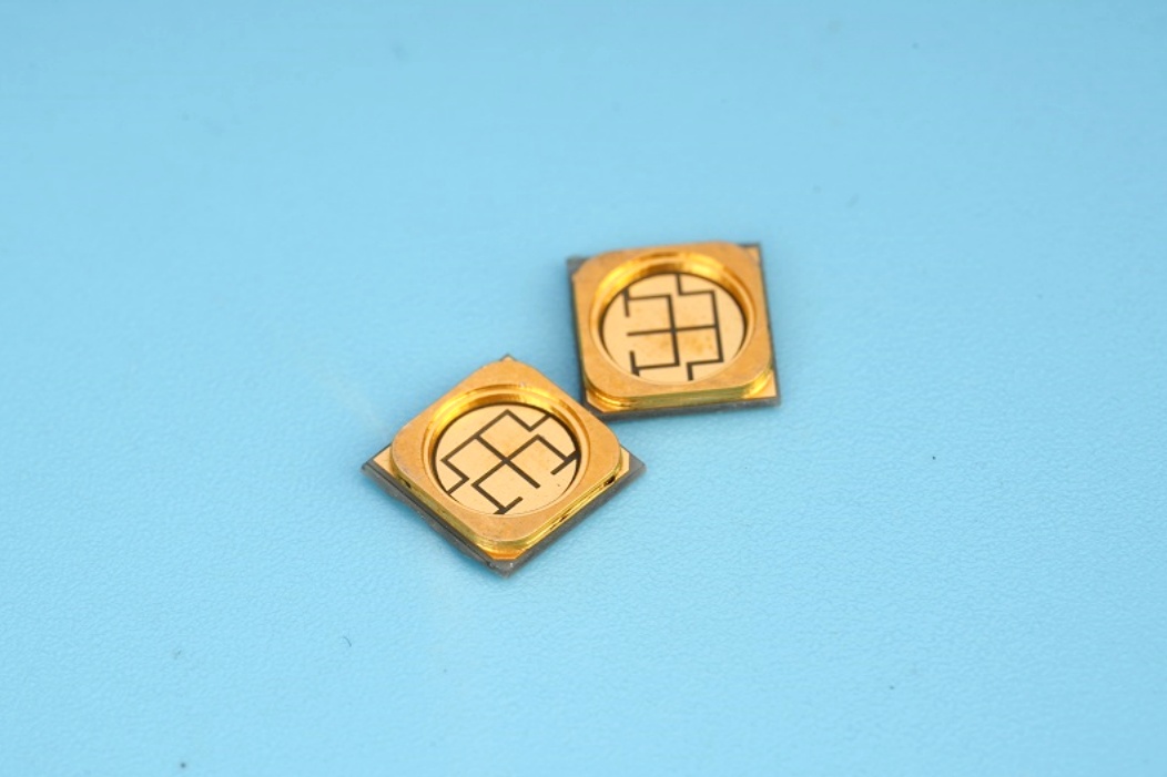
Direct Plated Copper (DPC) Ceramic PCB
DPC is a newer ceramic PCB process that offers excellent precision and strong metal adhesion. It starts with a thin seed layer of copper deposited via sputtering, followed by electroplating to build up the desired copper thickness. Laser or photolithographic methods define the circuit patterns.
Advantages:
- High precision with clean, fine traces
- Strong copper-to-ceramic bond
- Suitable for high-density, high-power circuits
Considerations:
- More complex and expensive than thick film
- Not ideal for ultra-thick copper layers (typically <100μm)
- DPC is ideal for high-power LED PCBs, power modules, and advanced RF components.
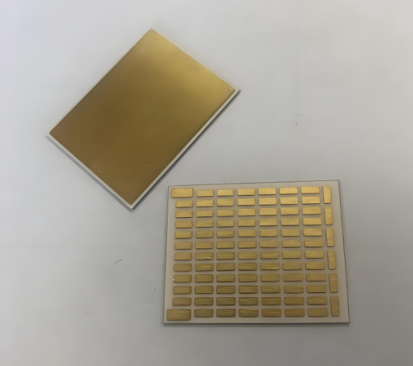
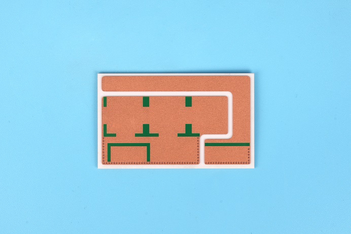
Direct Bonded Copper (DBC) Ceramic PCB
DBC is a process where thick copper sheets are directly bonded to ceramic substrates (such as Al₂O₃ or AlN) at high temperatures. A special oxidation process allows the copper to adhere to the ceramic without adhesives.
Advantages:
- Excellent thermal conductivity
- Thick copper layers (typically 200–800μm)
- Great for power electronics and modules
Considerations:
- Limited to relatively simple circuit patterns
- Higher copper usage increases material cost
You’ll commonly see DBC in IGBT modules, motor drives, and automotive inverters that need both electrical insulation and strong thermal performance.
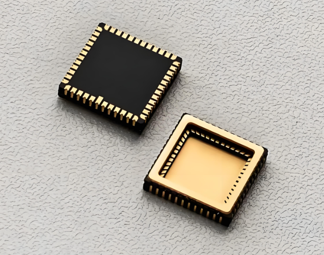
High-Temperature Co-fired Ceramic (HTCC) Ceramic PCB
HTCC involves printing metal pastes onto ceramic tape layers (usually alumina), stacking them, and then firing at temperatures above 1600°C to sinter everything together. Metals like tungsten or molybdenum are used due to their high melting points.
Advantages:
- Excellent mechanical strength
- Suitable for multilayer, hermetically sealed modules
- Good for aerospace and military electronics
Considerations:
- Complex and expensive process
- High sintering temperature limits metal choices
HTCC is ideal for high-reliability applications where ruggedness and environmental sealing are required.
Low-Temperature Co-fired Ceramic (LTCC) Ceramic PCB
LTCC ceramic PCB is similar to HTCC but uses glass-ceramic materials that sinter at lower temperatures (around 850°C). This allows the use of silver or gold as conductors, and makes integration of passive components easier.
Advantages:
- Supports multilayer, embedded circuits
- Lower cost than HTCC for certain designs
- Good RF and high-frequency performance
Considerations:
- Limited thermal conductivity compared to DBC or DPC
- Not suitable for very high-power applications
LTCC is widely used in telecommunications, radar modules, and compact RF devices.
Active Metal Brazed (AMB) Ceramic PCB
AMB metallization process involves attaching thick copper foil to ceramic using a reactive brazing alloy at temperatures around 900°C. Titanium-based braze alloys react with the ceramic to create a strong mechanical and thermal bond.
Advantages:
- Strongest copper-to-ceramic adhesion
- Excellent for high-current, high-voltage applications
- High reliability under thermal cycling
Considerations:
- Expensive materials and processing
- Less commonly available than DBC or DPC
AMB is preferred in high-voltage power electronics like railway traction inverters, industrial drives, and power distribution systems.
Comparison Table Between Them
|
Process |
Key Materials |
Cost Level |
Strengths |
Best for |
|
Thick Film |
Alumina + Ag/Au paste |
Low |
Simple, cost-effective |
Sensors, LEDs |
|
Thin Film |
Al₂O₃ + Au/Pt |
High |
High precision |
RF, optical |
|
DPC |
AlN/Al₂O₃ + Copper |
Medium-High |
Fine features, good thermal |
LED, RF |
|
DBC |
AlN/Al₂O₃ + Thick Copper |
Medium |
High power, thermal path |
IGBT, power modules |
|
HTCC |
Alumina + Mo/W |
High |
Multilayer, hermetic |
Military, aerospace |
|
LTCC |
Glass-ceramic + Ag/Au |
Medium |
Multilayer, embedded components |
RF, radar |
|
AMB |
AlN + Cu + Ti braze |
High |
High adhesion, thermal shock resistance |
Power, traction |
Which Metallization Method Is Right for You?
Selecting the right ceramic PCB process comes down to your application’s needs—thermal performance, layer count, circuit density, and budget all play a role. For example:
- Need high thermal conductivity and thick copper? Go with DBC or AMB.
- Require a compact, multilayer solution for RF? LTCC is a great fit.
- Looking for low-cost, simple circuits? Thick film might be all you need.
At Best Technology, we offer a full range of ceramic PCB solutions—from DPC and DBC to HTCC and LTCC—backed by professional engineering support and ISO-certified quality systems. Whether you're building a ceramic PCB prototype or scaling to mass production, we’re here to help you choose the most cost-effective and reliable option for your design.
 Products
 About us
 Contact us


