


 HOME
HOME

-

Silicon Nitride Substrate, Silicon Nitride Ceramic Substrate Formula
2025 05,08 -
How to choose the appropriate substrate for ceramic circuit boards?
2023 11,16 -
Laser Cutting or Water Saw Cutting? How To Choose the Best Cutting Solution for Ceramic Circuit Boards
2023 11,13 -
Why Ceramic PCB Is So Expensive?
2023 11,10 -
Which Process Ceramic Circuit Board Is A Better Solution For Semiconductor Refrigerator Chips?
2023 11,06 -
Silicon Printing Circuit Boards For Advancing Electronics
2023 10,27 -
What is the Difference Between HTCC and LTCC Ceramic PCB
2023 10,06 -
What is the Difference Between 96% and 99% Aluminum Oxide in Ceramic PCBs?
2023 09,20 -
Why thick film ceramic PCB is good for oil level sensor in automotive industry?
2023 08,25 -
Statistical analysis of ceramic PCB application fields
2023 08,16 -
Notice of anti-static requirements for PCBA processing and production
2023 08,16 -
Silver Paste: The Best Conductor Material for Via Holes in Thick Film Ceramic Boards
2023 08,16 -
Testing Circuit Board Ceramic Diode Fuses: A Complete Guide
2023 08,07 -
Why DBC is replaced by DPC in ceramic PCB manufacturing?
2023 08,01 -
What is thick film ceramic PCB?
2023 08,02
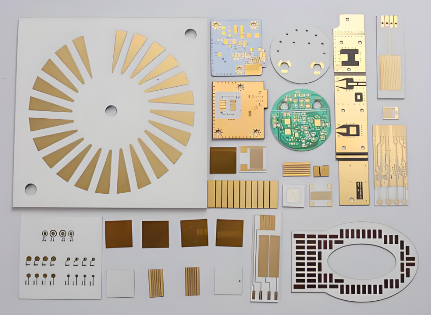
Ceramic PCB Materials, Types, and Advantages
A ceramic PCB is not just another printed circuit board—it's designed for demanding environments where heat, frequency, and reliability matter most. These boards use a ceramic PCB substrate like alumina or aluminum nitride to provide superior electrical insulation and heat transfer. In this guide, we’ll break down what ceramic PCBs are, how they work, and why they’re becoming so popular across high-tech industries.
What Is a Ceramic Circuit Board?
A ceramic circuit board is a type of PCB built on an inorganic ceramic substrate instead of traditional FR4. These substrates, such as alumina substrate or aluminum nitride, offer high thermal conductivity, excellent mechanical stability, and low dielectric loss. This makes ceramic boards ideal for high-power or high-frequency applications where standard boards fall short.
Common Ceramic PCB Materials
There are a few popular materials used as the base for ceramic PCB substrates:
- Alumina (Al₂O₃): The most widely used ceramic base. It offers a great balance between cost and ceramic PCB thermal conductivity, typically around 24 W/m·K.
- Aluminum Nitride (AlN): A premium material with higher thermal performance (over 170 W/m·K).
- Beryllium Oxide (BeO): Rarely used due to its toxicity, but it offers excellent heat dissipation.
Here is a table listing for better understanding and make a comparison:
|
Ceramic PCB Substrate |
Thermal Conductivity (W / m·K) |
Dielectric Constant (1 MHz) |
Typical Uses |
Key Strengths |
|
Alumina (Al₂O₃) |
≥ 24 W/m·K |
9 – 10 |
LED modules, general power boards |
Affordable, good all‑rounder |
|
Aluminum Nitride (AlN) |
≥ 170 W/m·K |
≈ 8.5 – 9 |
High‑power inverters, RF & microwave |
Very high heat transfer, CTE matched to Si |
|
Beryllium Oxide (BeO) |
≈ 260 – 285 W/m·K |
≈ 6.5 – 7 |
Laser drivers, aerospace & defense |
Highest conductivity; requires strict safety controls |
|
Silicon Nitride (Si₃N₄) |
≈ 90 W/m·K |
7.8 |
EV power modules, harsh‑environment electronics |
Tough, excellent thermal‑shock resistance |
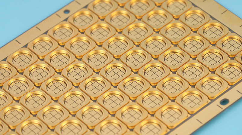
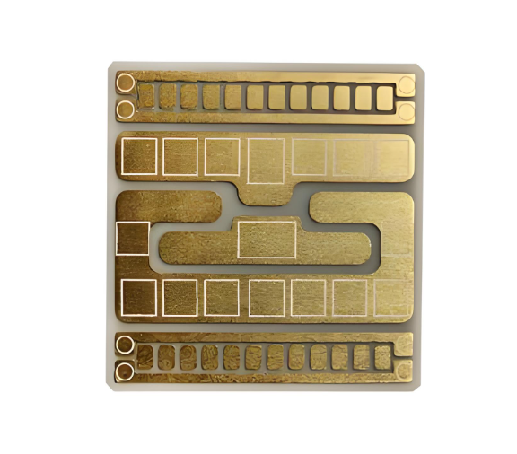
Types of Ceramic PCB Metallization Technologies
Ceramic PCBs can be manufactured using several different techniques, each offering unique performance advantages depending on the application. The three most widely used ceramic PCB technologies are:
- DBC (Direct Bonded Copper)
This process bonds a thick layer of copper directly onto the ceramic substrate, such as an alumina substrate or aluminum nitride. The DBC method provides strong adhesion, high current-carrying capability, and excellent heat dissipation. It’s commonly used in power modules, automotive inverters, and industrial motor drives.
- DPC (Direct Plated Copper)
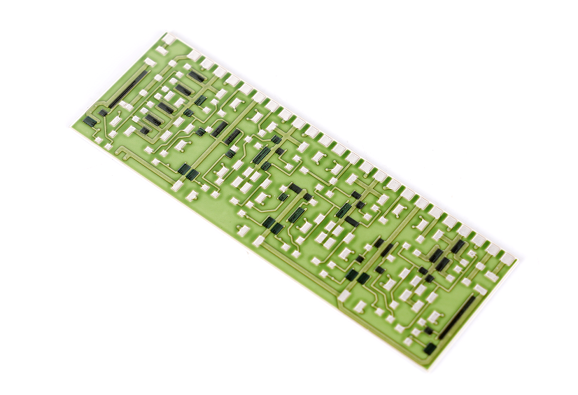
DPC uses a vacuum sputtering and electroplating process to form thin, precise copper traces on the ceramic surface. This technique supports finer line width/spacing and is ideal for high-frequency circuits and RF modules. It’s frequently chosen by advanced ceramic PCB manufacturers due to its compatibility with miniaturized components.
- Thick Film Ceramic PCB
In this method, conductive pastes (such as silver, gold, or copper) are screen printed onto the ceramic and then fired at high temperatures. This forms a durable yet flexible circuit layer. Though it offers lower conductivity compared to DBC or DPC, thick film ceramic boards are cost-effective for sensors, heaters, and hybrid microelectronics.
There are some other technologies like thin film, HTCC, LTCC, AMB to make the ceramic circuit board, but they are rarely to use and relatively expensive.
How Do Ceramic PCBs Work?
A ceramic PCB moves heat away from components by turning the whole ceramic pcb substrate into a wide, low‑resistance thermal highway. Copper traces or planes bonded by the ceramic pcb manufacturing process sit just microns above a crystal lattice that conducts heat 10 – 500 × faster than FR‑4.
- Three‑dimensional heat flow – Heat spreads laterally through the copper and vertically through the substrate, so hotspots flatten out quickly.
- Stable dielectric – Low, consistent εr keeps impedance predictable up to millimeter‑wave bands, crucial for 5 G, radar, and sat‑com.
- Low CTE mismatch – Alumina, AlN, and Si₃N₄ expand at rates close to silicon dies, reducing solder fatigue during power cycling.
- Mechanical backbone – Fine‑grain ceramics resist creep and maintain flatness, supporting heavy power semiconductors without bowing.
The result is a board that survives 200 °C junction temps, multi‑GHz edge rates, and 10 kV insulation stress—exactly why critical designers team with a seasoned ceramic pcb manufacturer.
Ceramic PCB vs. FR4: What's the Difference?
While FR4 boards are common in consumer electronics, they struggle with heat and signal losses. Ceramic boards resist high temperatures, manage power more efficiently, and maintain signal integrity in high-speed applications.
|
Feature |
Ceramic PCB |
FR‑4 PCB |
Impact on Design |
|
Thermal Conductivity |
24 – 285 W/m·K (Al₂O₃⇢BeO) |
~ 0.3 W/m·K |
Ceramic boards dissipate heat 80‑900 × faster. You need fewer vias, smaller heatsinks. |
|
Dielectric Loss (10 GHz) |
0.0001 – 0.0005 |
0.014 |
Lower insertion loss means cleaner RF, shorter trace lengths. |
|
Operating Temp |
≥ 250 °C |
≈ 130 °C |
Ceramic survives reflow‑like temps during service; FR‑4 chars. |
|
CTE (ppm/°C) |
4.8 – 8.5 |
14 – 17 |
Better chip‑to‑substrate match ⇒ higher solder joint life. |
|
Cost |
Higher material + process |
Low |
Use ceramics when performance or lifetime ROI exceeds the premium. |
Why Choose a Ceramic PCB?
One major reason engineers turn to ceramic PCBs is heat dissipation. The high thermal conductivity of materials like aluminum nitride allows heat to spread quickly away from heat-sensitive components. Ceramic boards also have a very low coefficient of thermal expansion, which minimizes stress between the PCB and mounted components—an important advantage when using materials like silicon carbide or gallium nitride.
In high-frequency applications, the consistent dielectric properties of ceramic substrates ensure stable impedance and low signal loss. That’s why ceramic PCBs are increasingly used in 5G systems, radar modules, and RF amplifiers.
For industries like aerospace, automotive, or medical, working with an experienced ceramic PCB manufacturer ensures you get precision, performance, and consistency. Whether you need prototypes or high-volume production, ceramic circuit boards offer a dependable solution when standard FR4 boards simply aren't enough.
Frequently Asked Questions
1. What is the thermal conductivity of a ceramic PCB?
The thermal conductivity depends on the material used. Alumina offers around 24 W/m·K, while aluminum nitride can exceed 170 W/m·K. If your application demands even more heat transfer, beryllium oxide delivers over 250 W/m·K—but it requires careful handling due to safety concerns.
2. Can I design multilayer ceramic PCBs?
Yes, multilayer ceramic PCBs are available through technologies like LTCC, HTCC, and stacked thick film processes. They allow designers to create complex circuits in compact formats while still benefiting from the mechanical and thermal properties of ceramic substrates.
3. Is it possible to add microvias on ceramic PCBs?
In many cases, yes. Technologies like laser drilling in DPC processes support blind vias, although not all ceramic board types—especially thick film—are suitable for them. Design rules depend on the manufacturer’s capabilities, so always consult early.
4. Are ceramic PCBs compliant with environmental and safety regulations?
Most ceramic PCB substrates like alumina, aluminum nitride, and silicon nitride are naturally RoHS compliant and meet UL standards for flammability. However, beryllium oxide, while high-performing, requires special consideration due to its toxic dust risk during processing.
5. How fast can I receive a prototype from a ceramic PCB manufacturer?
Turnaround time depends on the complexity of your design and the specific ceramic PCB manufacturing process used. For standard DPC or DBC-based prototypes, experienced manufacturers can typically deliver samples within 10 to 15 business days.
 Products
 About us
 Contact us


