


 HOME
HOME

-

Wire bondable 2-layer Alumina substrates PCB | Bstceramic PCB
2025 09,22 -
Silicon Nitride Substrate, Silicon Nitride Ceramic Substrate Formula
2025 05,08 -
How to choose the appropriate substrate for ceramic circuit boards?
2023 11,16 -
Laser Cutting or Water Saw Cutting? How To Choose the Best Cutting Solution for Ceramic Circuit Boards
2023 11,13 -
Why Ceramic PCB Is So Expensive?
2023 11,10 -
Which Process Ceramic Circuit Board Is A Better Solution For Semiconductor Refrigerator Chips?
2023 11,06 -
Silicon Printing Circuit Boards For Advancing Electronics
2023 10,27 -
What is the Difference Between HTCC and LTCC Ceramic PCB
2023 10,06 -
What is the Difference Between 96% and 99% Aluminum Oxide in Ceramic PCBs?
2023 09,20 -
Why thick film ceramic PCB is good for oil level sensor in automotive industry?
2023 08,25 -
Statistical analysis of ceramic PCB application fields
2023 08,16 -
Notice of anti-static requirements for PCBA processing and production
2023 08,16 -
Silver Paste: The Best Conductor Material for Via Holes in Thick Film Ceramic Boards
2023 08,16 -
Testing Circuit Board Ceramic Diode Fuses: A Complete Guide
2023 08,07 -
Why DBC is replaced by DPC in ceramic PCB manufacturing?
2023 08,01 -
What is thick film ceramic PCB?
2023 08,02
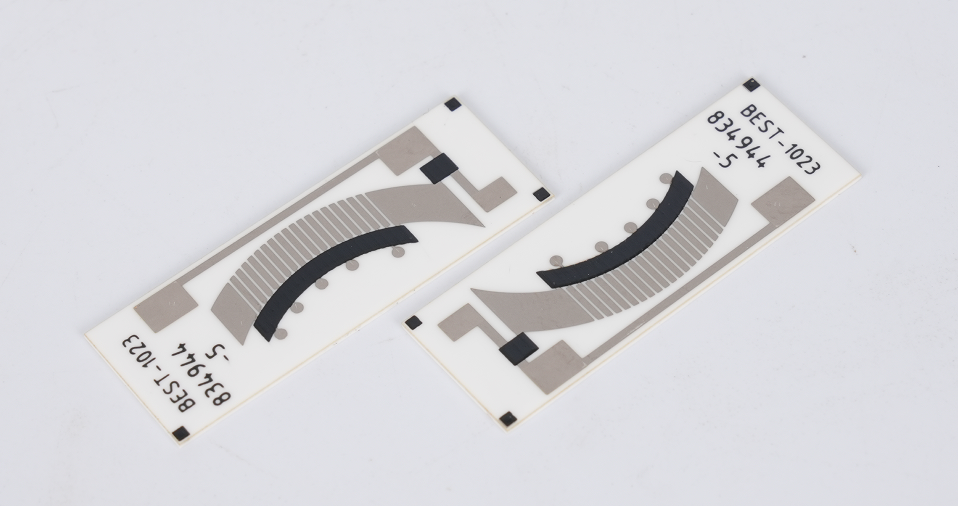
Hybrids Thick Film Ceramic PCB for Fuel Sensors
Hybrid thick film ceramic PCBs have become a cornerstone in automotive sensor technology. Fuel sensors, in particular, require PCBs that can withstand high temperatures, vibration, and chemical exposure. Hybrid designs combine the robustness of ceramic substrates with thick film technology, creating precise, reliable circuits. These PCBs deliver both electrical performance and mechanical strength, making them ideal for modern fuel sensors.
With automotive applications pushing limits in performance and safety, choosing the right PCB design is crucial. Hybrid thick film ceramic PCBs offer the durability, stability, and miniaturization needed to meet these demands.
What is a Hybrid Thick Film Ceramic PCB?
A hybrid thick film ceramic PCB is a printed circuit board built on a ceramic substrate with thick film technology applied for circuitry. Unlike conventional FR4 PCBs, which use epoxy laminates, ceramic PCBs use materials such as alumina (Al₂O₃) or aluminum nitride (AlN). These materials provide excellent thermal conductivity and high-temperature resistance.
In thick film technology, conductive, resistive, and dielectric pastes are screen-printed onto the ceramic substrate. These pastes are then fired at high temperatures, creating robust, durable circuit patterns. Hybrid PCBs integrate multiple materials and layers, combining different properties to achieve better performance in extreme conditions.
Compared to thin film PCBs, thick film circuits allow for higher current capacity and mechanical strength, making them ideal for automotive and industrial sensors.
Why Use Hybrid Ceramic PCBs in Fuel Sensors?
Hybrid ceramic PCBs are increasingly used in fuel sensors because these sensors operate under extreme environmental conditions. Standard FR4 boards fail to maintain accuracy under high temperatures, chemical exposure, and mechanical stress. Ceramic-based hybrid PCBs solve these problems while offering precise electrical performance.
- High Thermal Stability
Fuel sensors are often located near engine components, where ambient temperatures can reach 150–250°C, and transient spikes can hit 400–500°C. Ceramic substrates such as alumina (Al₂O₃) can withstand continuous temperatures of up to 450°C. Aluminum nitride (AlN) substrates perform even better with thermal conductivity up to 170 W/m·K, compared to alumina's ~24 W/m·K. This helps dissipate heat efficiently and maintain sensor reliability.
- Electrical Performance and Accuracy
Thick film resistors on hybrid ceramic PCBs maintain low temperature coefficients of resistance (TCR). For instance, a thick film resistor on alumina can have a TCR as low as ±50 ppm/°C, ensuring minimal drift in fuel measurement. Low parasitic capacitance (<1 pF/mm) also helps maintain signal integrity in sensitive analog circuits.
- Mechanical Durability
Fuel sensors experience constant vibration and occasional mechanical shocks. Ceramic PCBs exhibit high Young’s modulus (~350 GPa for alumina), providing mechanical rigidity. This prevents circuit cracks and maintains long-term sensor accuracy.
- Chemical Resistance
Exposure to gasoline, diesel, and ethanol blends can degrade conventional PCBs. Alumina and AlN are chemically inert, resisting corrosion and maintaining performance even after prolonged contact with fuels.
- Miniaturization and Integration
Hybrid thick film technology allows integration of resistors, capacitors, and conductive paths in a compact space. For fuel sensors, where PCB dimensions are often <20 x 20 mm, hybrid designs allow dense layouts without compromising performance.
Design Considerations for Fuel Sensor PCBs
Designing hybrid thick film ceramic PCBs for fuel sensors requires a balance of electrical performance, thermal management, and mechanical strength.
1. Substrate Selection
- Alumina (Al₂O₃): Common, cost-effective, continuous temperature up to 450°C, thermal conductivity ~24 W/m·K.
- Aluminum Nitride (AlN): Expensive, higher thermal conductivity (~170 W/m·K), ideal for high-power or densely populated circuits.
- Thickness: 0.254–1.0 mm is common for compact sensor designs. Thinner substrates improve heat transfer to sensor housing.
2. Thick Film Material Choices
- Conductive Pastes: Silver-palladium or gold pastes for high conductivity and chemical resistance. Conductivity typically 10⁶–10⁷ S/m.
- Resistive Pastes: For integrated resistors with TCR ±50–100 ppm/°C. Resistance range 10 Ω–1 MΩ.
- Dielectric Pastes: Provide insulation between layers; dielectric constant typically 6–9, allowing stable signal routing.
3. Circuit Layout and Signal Integrity
- Keep sensitive analog traces away from high-current paths to avoid interference.
- Impedance control is critical for circuits interfacing with microcontrollers or ADCs in fuel sensors.
- Use ground planes to reduce noise; for example, a 0.5 mm thick alumina substrate can support a continuous ground plane with minimal thermal expansion effects.
4. Thermal Management
- Placement of power-dissipating components near high thermal conductivity areas.
- Consider vias or thick copper for heat spreading; thermal via density ~50–100 vias/cm² can reduce hotspot temperature by 20–30°C.
5. Size and Packaging Constraints
- Typical fuel sensor PCBs are compact: 15–25 mm².
- Components must be low-profile (<1 mm) to fit within the sensor housing.
- Hybrid thick film technology allows integrating resistors and capacitors directly on the PCB, reducing assembly complexity.
6. Reliability Standards
- Automotive sensors must meet AEC-Q200 standards for passive components.
- Thermal cycling tests: -40°C to 150°C for 1000+ cycles to ensure dimensional and electrical stability.
Manufacturing Process of Hybrid Thick Film Ceramic PCBs
The manufacturing of hybrid thick film ceramic PCBs is a precise process that combines material science and advanced production techniques.
1. Substrate Preparation
The process begins with selecting high-quality ceramic substrates, commonly alumina (Al₂O₃) or aluminum nitride (AlN), depending on thermal requirements. The substrate is cut to precise dimensions, typically 0.254–1.0 mm thick, and polished to achieve a smooth, flat surface. Proper flatness and surface finish are critical to ensure uniform adhesion of thick film pastes and to prevent defects during firing. Substrate tolerances are carefully controlled, usually ±25 μm for thickness and ±50 μm for XY dimensions, to maintain consistency across production batches.
2. Thick Film Printing
After substrate preparation, conductive, resistive, and dielectric pastes are applied using screen printing or stencil printing. Each layer is printed separately, and precise alignment is critical, especially for multi-layer designs. Conductive pastes (e.g., silver-palladium or gold) form the electrical pathways, while resistive pastes create integrated resistors with precise values. Dielectric pastes provide insulation between layers. Typical line widths range from 0.1–0.2 mm, with minimum spacing around 0.1 mm, depending on paste properties and printing resolution.
3. Firing Process
Once the thick film pastes are printed, the board undergoes firing in a high-temperature kiln. Firing temperatures are generally 850–900°C for alumina and 900–1000°C for aluminum nitride. This step sinters the pastes, bonding them permanently to the ceramic substrate. Co-firing may be used for multi-layer boards, allowing multiple layers to be integrated in a single firing cycle. The firing process not only solidifies the printed patterns but also ensures excellent electrical conductivity, mechanical adhesion, and long-term thermal stability.
4. Post-Processing and Trimming
After firing, the hybrid PCB undergoes post-processing to fine-tune its electrical properties. Integrated resistors are often laser-trimmed to achieve precise resistance values, usually within ±1% tolerance. Through-holes or metallized vias are added for interlayer connections. This stage may also involve adding protective coatings or assembling discrete components, such as SMD resistors or capacitors, directly onto the board. Post-processing ensures that the PCB meets exact design specifications and is ready for functional testing.
5. Quality Control and Testing
The final step focuses on comprehensive inspection and testing to guarantee reliability. Electrical tests verify continuity, insulation resistance, and the accuracy of resistor values. Thermal cycling tests simulate automotive operating conditions, typically ranging from -40°C to 150°C for 1000 cycles, to confirm stability under extreme conditions. Mechanical inspections detect any cracks, warping, or delamination. Only boards that pass strict quality criteria move on to assembly or shipment, ensuring long-term performance in fuel sensors and other demanding applications.
Advantages of Hybrid Thick Film Ceramic PCBs for Fuel Sensors
- High-Temperature Tolerance: They perform reliably in environments up to 850°C.
- Mechanical Strength: Resistance to vibration and thermal epansion prevents cracks.
- Chemical Resistance: Ceramics are impervious to fuel, oils, and corrosive gases.
- Stable Electrical Characteristics: Thick film resistors maintain accuracy over long periods.
- Miniaturization: Hybrid designs allow dense circuit layouts in compact sensor housings.
Applications Beyond Fuel Sensors
While fuel sensors are a primary application, hybrid thick film ceramic PCBs are used in multiple fields:
- Automotive Sensors: Oil, temperature, and pressure sensors benefit from thermal and chemical resistance.
- Industrial Sensors: Harsh environments, such as chemical plants or heavy machinery, require durable PCBs.
- Aerospace and Military: Critical sensors demand precision, stability, and reliability under extreme conditions.
The combination of ceramic substrates and thick film technology ensures consistent performance across industries.
FAQs
1. What is the maximum operating temperature of a hybrid thick film ceramic PCB?
Up to 500°C, depending on substrate material and design.
2. How does thick film technology enhance fuel sensor performance?
It provides stable resistors and precise conductive paths that resist temperature and chemical effects.
3. Can hybrid ceramic PCBs be used in other automotive sensors?
Yes, they are suitable for oil, pressure, and temperature sensors.
4. What are the main differences between thick film and thin film ceramic PCBs?
Thick film offers higher current capacity and mechanical durability, while thin film is better for ultra-precise microcircuits.
5. How do manufacturers ensure long-term reliability in fuel sensor PCBs?
Through careful material selection, controlled firing, post-processing adjustments, and comprehensive quality testing.
 Products
 About us
 Contact us


