


 HOME
HOME

-

Wire bondable 2-layer Alumina substrates PCB | Bstceramic PCB
2025 09,22 -
Silicon Nitride Substrate, Silicon Nitride Ceramic Substrate Formula
2025 05,08 -
How to choose the appropriate substrate for ceramic circuit boards?
2023 11,16 -
Laser Cutting or Water Saw Cutting? How To Choose the Best Cutting Solution for Ceramic Circuit Boards
2023 11,13 -
Why Ceramic PCB Is So Expensive?
2023 11,10 -
Which Process Ceramic Circuit Board Is A Better Solution For Semiconductor Refrigerator Chips?
2023 11,06 -
Silicon Printing Circuit Boards For Advancing Electronics
2023 10,27 -
What is the Difference Between HTCC and LTCC Ceramic PCB
2023 10,06 -
What is the Difference Between 96% and 99% Aluminum Oxide in Ceramic PCBs?
2023 09,20 -
Why thick film ceramic PCB is good for oil level sensor in automotive industry?
2023 08,25 -
Statistical analysis of ceramic PCB application fields
2023 08,16 -
Notice of anti-static requirements for PCBA processing and production
2023 08,16 -
Silver Paste: The Best Conductor Material for Via Holes in Thick Film Ceramic Boards
2023 08,16 -
Testing Circuit Board Ceramic Diode Fuses: A Complete Guide
2023 08,07 -
Why DBC is replaced by DPC in ceramic PCB manufacturing?
2023 08,01 -
What is thick film ceramic PCB?
2023 08,02
Wire bondable 2-layer Alumina substrates PCB | Bstceramic PCB
As electronic systems evolve toward higher power density, miniaturization, and long-term reliability, traditional FR4 or metal-core PCBs often fail to meet the requirements. Wire bondable 2-layer alumina substrates PCB provides a solution that combines ceramic stability, wire bonding compatibility, and multilayer routing, making it ideal for applications such as LED modules, RF circuits, power electronics, and sensors.
In this article, we’ll explore the structure, materials, advantages, applications, and engineering considerations of wire bondable alumina PCBs, and why industries increasingly rely on them.
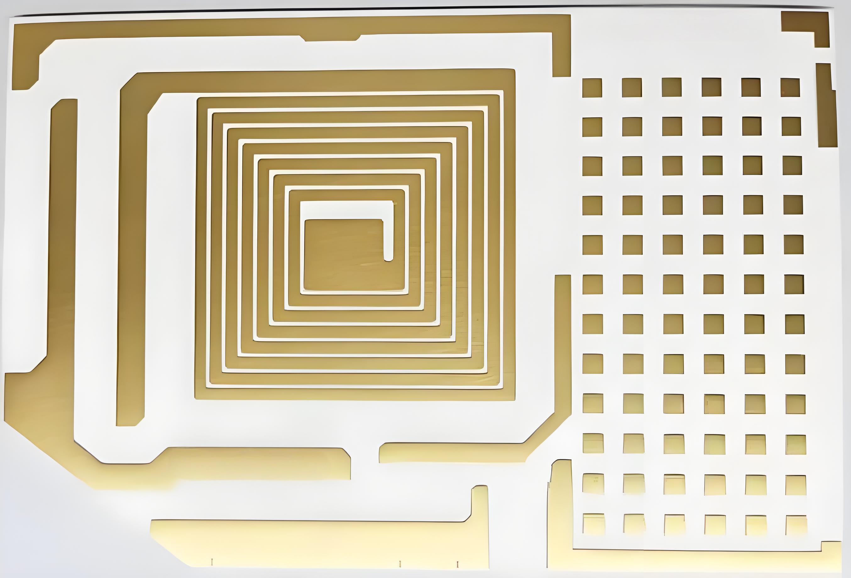
What Is a Wire Bondable 2-Layer Alumina Substrate PCB?
A wire bondable 2-layer alumina substrate PCB is a ceramic-based printed circuit board made primarily of alumina (Al₂O₃). The two layers typically consist of metal traces on the top and bottom surfaces of the ceramic base. “Wire bondable” refers to the board’s ability to allow ultrasonic or thermosonic wire bonding, which connects chips, LEDs, or sensors directly to the conductive pads.
This PCB type combines mechanical robustness, high thermal conductivity, and low dielectric loss, making it suitable for applications where precision and heat dissipation are essential. Unlike conventional PCBs, alumina substrates can handle higher currents, elevated temperatures, and harsh environmental conditions.
Materials Used in Wire Bondable Alumina PCBs
1. Alumina Substrate (Al₂O₃)
The core of the board is alumina ceramic, typically 96–99.6% pure. Alumina provides:
- High thermal conductivity for efficient heat dissipation.
- Excellent electrical insulation to prevent shorts.
- Mechanical strength to resist warping or cracking.
- Chemical stability, which protects against corrosion or environmental damage.
2. Metallization Layers
The conductive layers on top and bottom are usually made of silver, copper, or gold. For wire bonding, gold or palladium-gold plating is common because it ensures strong and reliable bonds without corrosion.
3. Dielectric Layers (Optional)
Some designs incorporate sintered dielectric layers to separate conductive layers or allow vias and interconnects between the two layers. These layers must be compatible with the ceramic’s thermal expansion to avoid stress fractures.
Features of Alumina Substrate PCB
- Superior Thermal Management: Alumina spreads heat efficiently, protecting sensitive high-power devices.
- Wire Bonding Compatibility: Gold or Pd/Au pads ensure reliable bonding for LEDs, ICs, and MEMS devices.
- High Temperature Tolerance: Operational stability above 350°C, and short-term resistance up to 1000°C.
- Mechanical Robustness: Resists warping, cracking, and thermal cycling.
- Low Dielectric Loss: Maintains signal integrity for RF, microwave, and high-speed circuits.
Applications of Wire Bondable 2-Layer Alumina Substrates
Wire bondable alumina PCBs are widely used across industries due to their thermal stability, wire bonding capability, and electrical performance:
- Automotive headlights
- Industrial lighting
- UV curing lamps, outdoor displays
- 5G base stations
- Satellite communications
- Radar modules
- Motor drivers
- IGBT/SiC MOSFET modules
- Implantable sensors
- Diagnostic imaging modules
- Avionics, missile guidance systems
- Integrates wire-bonded dies and SMT components
- Pressure sensors, gyroscopes
- Infrared sensors
Wire Bondable Alumina PCB Design Considerations
When designing wire bondable 2-layer alumina PCBs, engineers must carefully balance thermal, electrical, and mechanical requirements. Each factor directly influences the final reliability and performance of the product.
- Pad Metallization and Surface Quality
A smooth surface and proper metallization are essential for wire bonding. Gold layers with a thickness of 3–5 µm are typically applied to achieve stable bonds, while a surface roughness (Ra) of ≤0.1 µm helps ensure uniform adhesion.
- Trace Width and Spacing
Copper trace geometry should be defined based on current load and frequency response. For power circuits, trace widths above 200 µm are recommended, while RF lines must maintain impedance control within ±5% to ensure signal integrity.
- Thermal Management
Alumina’s thermal conductivity of 20–24 W/m·K is significantly higher than FR4. Designers often incorporate thermal vias (≥0.2 mm) or backside metallization to spread heat evenly, particularly in power modules or LED applications.
- Via Design
Conductive-filled vias improve both electrical and thermal performance. For mechanical stability, aspect ratios should not exceed 8:1, preventing stress fractures during operation and thermal cycling.
- Layer Alignment
Precise alignment between the two layers is critical in dense circuits. Tolerances are usually kept within ±25 µm, as even minor misalignment can affect impedance and bonding pad registration.
- Wire Bonding Process Compatibility
Alumina substrates must be designed with bonding forces and pull strengths in mind. For example, 25 µm gold wire typically requires ultrasonic bonding forces of 30–120 g, and a minimum pull strength of 7 g in accordance with MIL-STD-883 standards.
Why Choose Alumina for Wire Bondable PCBs?
Alumina (Al₂O₃) has become the preferred material for wire bondable PCBs because it offers an optimal balance of thermal, mechanical, and electrical properties while remaining cost-effective. Compared with traditional FR4 and high-end ceramic alternatives such as Aluminum Nitride (AlN), alumina delivers superior performance in demanding environments.
|
Property / Feature |
Alumina (Al₂O₃) |
FR4 (Epoxy/Glass) |
Aluminum Nitride (AlN) |
|
Thermal Conductivity (W/m·K) |
20 – 24 |
~0.3 |
170 – 200 |
|
Continuous Operating Temp (°C) |
>350 |
<150 |
>400 |
|
Dielectric Constant (1 MHz) |
9.8 – 10.2 |
4.2 – 4.8 |
8.6 – 9.0 |
|
Dielectric Loss Tangent |
0.0001 – 0.0005 |
0.02 |
0.0003 |
|
Thermal Expansion (ppm/°C) |
~7 |
~16 |
~4.5 |
|
Flexural Strength (MPa) |
~350 |
~450 |
~300 |
|
Wire Bonding Compatibility |
Excellent (Au/Al) |
Poor |
Excellent (Au/Al) |
|
Thermal Shock Resistance |
Good (ΔT >150°C) |
Poor |
Excellent (ΔT >200°C) |
|
Hermeticity |
High (gas tight) |
Low |
High |
|
Chemical Resistance |
Excellent |
Moderate |
Excellent |
|
Market Availability |
Widely Available |
Very High |
Limited (high cost) |
|
Cost Level |
Medium |
Low |
High |
From the above, it is clear that alumina offers thermal and electrical advantages far superior to FR4, while providing better cost-efficiency than AlN. This balance makes alumina the most practical choice for high-power, RF, and wire-bonding applications where performance and affordability must coexist.
Best Technology’s Advantage in Alumina PCB Manufacturing
At Best Technology, we deliver high-performance alumina PCBs that meet the toughest requirements in LEDs, RF circuits, sensors, and power electronics.
Our advantages include:
- Over 19 years of ceramic PCB design & manufacturing experience
- DFM support for cost-effective layouts
- Options for thick film, thin film, DPC, DBC, AMB, HTCC, LTCC ceramic PCBs
- Flexible metallization choices (Au, Ag, Cu, Pd/Au)
- Thickness range: 0.25 mm – 2.0 mm.
- In-house ceramic processing reduces outsourcing costs.
- ISO9001, ISO13485, IATF16949, and AS9100D certificated
- 100% electrical and visual inspection before shipment
Partnering with Best Technology ensures durable, reliable, and application-optimized wire bondable PCBs.
FAQs
1. What makes a PCB “wire bondable”?
It uses special metallization (e.g., gold or Pd/Au) that allows direct ultrasonic or thermosonic bonding of fine wires.
2. Why is alumina better than FR4 for high-power applications?
Alumina has far higher thermal conductivity and temperature stability, ensuring reliable operation in harsh conditions.
3. Can alumina PCBs be used in RF designs?
Yes. Their low dielectric loss supports high-frequency and microwave applications.
4. What thickness options are available for 2-layer alumina PCBs?
Common thicknesses range from 0.25 mm to 1.0 mm, depending on thermal and mechanical requirements.
5. What bonding wires are typically used?
Gold and aluminum wires are most common, chosen based on application and cost.
The wire bondable 2-layer alumina substrates PCB combines the thermal performance of ceramics, the design flexibility of double layers, and the precision of wire bonding. It is the go-to choice for industries ranging from high-power LEDs and RF communication to sensors and hybrid microelectronics.
With the right design considerations and expert manufacturing, these PCBs provide unmatched performance and reliability.
Choosing Best Technology as your manufacturing partner guarantees access to advanced ceramic PCB solutions engineered for your toughest challenges.
 Products
 About us
 Contact us


