


 HOME
HOME

-

Silicon Nitride Substrate, Silicon Nitride Ceramic Substrate Formula
2025 05,08 -
How to choose the appropriate substrate for ceramic circuit boards?
2023 11,16 -
Laser Cutting or Water Saw Cutting? How To Choose the Best Cutting Solution for Ceramic Circuit Boards
2023 11,13 -
Why Ceramic PCB Is So Expensive?
2023 11,10 -
Which Process Ceramic Circuit Board Is A Better Solution For Semiconductor Refrigerator Chips?
2023 11,06 -
Silicon Printing Circuit Boards For Advancing Electronics
2023 10,27 -
What is the Difference Between HTCC and LTCC Ceramic PCB
2023 10,06 -
What is the Difference Between 96% and 99% Aluminum Oxide in Ceramic PCBs?
2023 09,20 -
Why thick film ceramic PCB is good for oil level sensor in automotive industry?
2023 08,25 -
Statistical analysis of ceramic PCB application fields
2023 08,16 -
Notice of anti-static requirements for PCBA processing and production
2023 08,16 -
Silver Paste: The Best Conductor Material for Via Holes in Thick Film Ceramic Boards
2023 08,16 -
Testing Circuit Board Ceramic Diode Fuses: A Complete Guide
2023 08,07 -
Why DBC is replaced by DPC in ceramic PCB manufacturing?
2023 08,01 -
What is thick film ceramic PCB?
2023 08,02
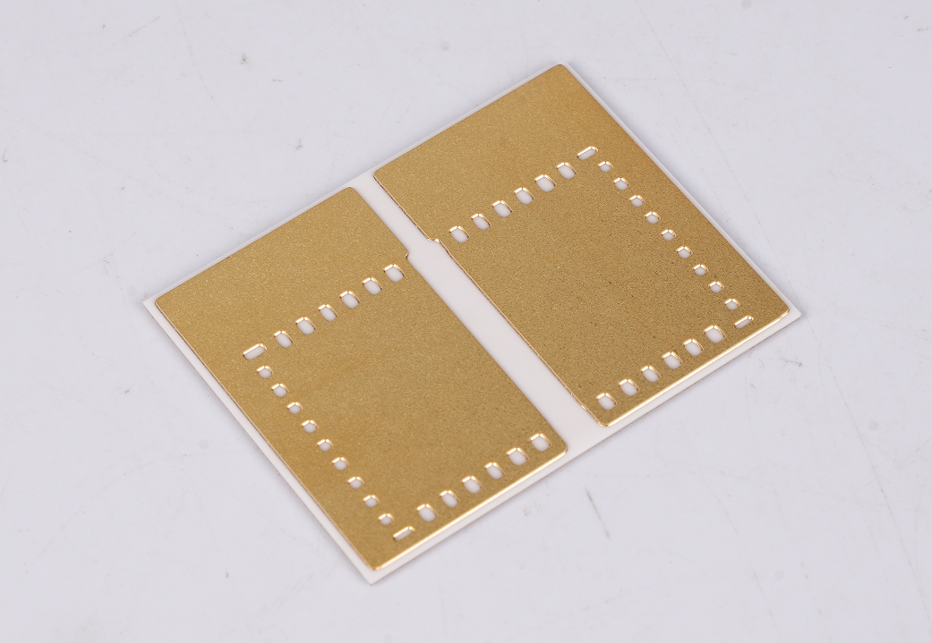
Thick Copper Direct Bond Copper DBC Ceramic Substrate
Direct bond copper (DBC) ceramic substrates play a key role in high-power electronics. When you need a solution that handles high voltage, high current, and heat — without compromising reliability — DBC is one of the top choices. Especially when combined with thick copper layers, these substrates support long-term performance in power devices, automotive systems, and industrial modules.
In this article, we’ll walk through what DBC ceramic substrates are, why copper thickness matters, how they’re made, and how they compare with similar technologies like AMB. If you're considering DBC for your design, this guide will help you understand the value of this substrate and how manufacturers like Best Technology support custom DBC solutions for different industries.
What Are Direct Bond Copper Substrates?
Direct bond copper substrates, or DBC substrates, are made by bonding a layer of pure copper directly onto a ceramic base. The ceramic provides strong electrical insulation and thermal conductivity, while the copper offers a solid, conductive surface for mounting electronic components.
Unlike standard PCB materials, these substrates don’t use adhesives or prepreg to hold copper and base material together. Instead, the copper is bonded through a high-temperature process that forms a durable oxide layer, ensuring long-term adhesion.
The main advantages of DBC ceramic substrates include:
- Excellent heat dissipation
- High current-carrying capacity
- Strong electrical insulation
- Reliable performance in harsh environments
Common ceramic materials used in DBC include Alumina (Al₂O₃), Aluminum Nitride (AlN), and Silicon Nitride (Si₃N₄). These offer different levels of thermal conductivity and mechanical strength, depending on application needs.
How Thick Is the Copper in DBC?
One major advantage of DBC substrates is the option to use thick copper layers. Typical copper thicknesses range from 100μm (3 oz) up to 600μm (18 oz), although special applications may go even higher. In contrast, DPC (direct plat copper) ceramic PCB can only plate 2um – 200um copper on its surface. So if your project requires 300um copper plating, you can only choose DBC metallization process and AMB process (but there is no mature AMB ceramic PCB manufacturer right now).
The thick copper thickness allows DBC substrates carry large currents without overheating or damaging traces. That’s why thick copper PCB designs are so popular in high-power circuits, like motor drivers, inverters, and power modules.
Thicker copper also allows for better heat spreading, which reduces the chance of hot spots forming around high-power components. As a result, you get improved thermal performance and increased product lifespan.
What Is the Difference Between DBC and AMB Substrate?
You may have also heard about AMB substrates, short for Active Metal Brazing. These are similar to DBC in that they also bond copper to a ceramic base. However, the bonding methods are different.
|
Feature |
DBC (Direct Bond Copper) |
AMB (Active Metal Brazing) |
|
Bonding Method |
Thermal oxidation and diffusion bonding |
Brazing with active metals (e.g., titanium) |
|
Temperature |
~1065–1083°C |
~850–900°C |
|
Copper Thickness |
100um – 600um |
250um – 800um |
|
Adhesion |
Good in most cases |
Excellent with strong ceramic bonds |
|
Materials |
Al₂O₃, AlN |
AlN, Si₃N₄ (mostly) |
|
Application |
General power electronics |
High-demand, thermal cycling, extreme conditions |
In short, DBC is more cost-effective and widely used in mid-range power modules, while AMB is preferred for extreme environments such as aerospace or long-life automotive inverters.
How to Bond Copper to Ceramic?
The process of bonding copper to ceramic in DBC substrates is precise and requires controlled conditions. Unlike lamination or adhesive-based bonding in regular PCBs, DBC uses direct metallurgical bonding. Here’s how it works:
- A clean ceramic wafer/substrate (e.g., AlN or Al₂O₃) is prepared.
- A sheet of oxygen-free copper is placed on top.
- The assembly is heated in a controlled oxygen environment.
- As temperature rises above 1065°C, copper begins to oxidize, forming Cu₂O (copper oxide).
- This oxide reacts with the ceramic surface, forming a strong chemical bond.
- The copper adheres directly to the ceramic without needing extra layers or glue.
This bonding process is permanent and can withstand mechanical stress, high voltage, and thermal cycling — which makes it perfect for power modules that go through frequent on/off switching or heavy load.
What Temperature Is Direct Copper Bonding?
The bonding temperature for DBC substrates is typically in the range of 1065°C to 1083°C, which is just below the melting point of copper. During the copper bonding process, maintaining the right temperature is crucial:
- Too low, and the copper oxide doesn’t form correctly.
- Too high, and the copper melts, leading to bonding failure or warping.
To control this, manufacturers use oxygen-controlled furnaces and carefully monitor heating rates and holding times. The result is a clean, uniform bond between the copper and the ceramic, which ensures long-term electrical and thermal performance.
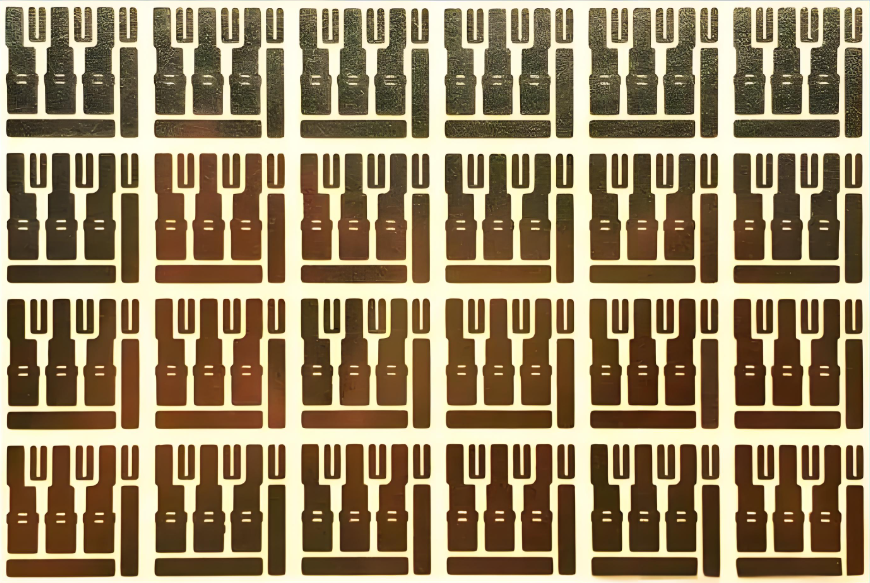
DBC Direct Bond Copper Process
Let’s take a closer look at the full DBC fabrication process, from raw materials to the finished substrate:
Step 1: Surface Preparation
Both copper and ceramic surfaces are cleaned to remove particles or oxidation that could interfere with bonding.
Step 2: Stacking and Alignment
The copper sheet is placed on top of the ceramic substrate in a precise alignment, ready for bonding.
Step 3: Direct Copper Bonding
The assembly is heated in a furnace with controlled oxygen levels to form the bond. The copper layer bonds tightly to the ceramic, forming a single substrate.
Step 4: Cooling
The bonded structure is cooled gradually to prevent stress or cracking.
Step 5: Post-Processing
The DBC substrate is now ready for:
- Drilling (via holes, mounting holes)
- Surface plating (Ni/Au, Ni/Ag, etc.)
- Pattern etching (circuit traces)
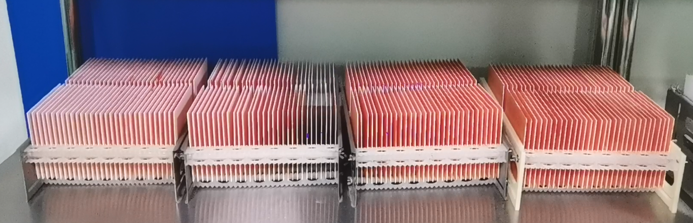
Please click here to view the detailed manufacturing process introduction. Manufacturers like Best Technology can also provide custom DBC layouts, gold plating for wire bonding, or solder mask for insulation.
Who Makes DBC Substrates?
Actually, several companies around the world specialize in producing DBC ceramic substrates, both standard and custom types. Global manufacturers like Best Technology in China, Rogers in USA, Heraeus electronics in Germany, Denka in Japan.
As one of the leading direct bond copper substrate manufacturers in China, Best Technology provides complete solutions for thick copper DBC ceramic substrates.
- We are ISO9001, IATF16949, and AS9100D certified
- Supports custom designs for automotive, industrial, and renewable energy sectors
- Offers fast production, technical support, and traceable material sourcing
- Providing COC report with the shipment
- Full turnkey service from alumina material cutting, manufacturing, assembly and testing
- Offers 5 years quality assurance to make you no worries
- One-on-one vip sales assistant support before and after sales
- WIP updates for every Wednesday and Friday
If you're developing high-power electronics, partnering with a supplier like Best Technology ensures consistent performance and professional support from prototype to volume production.
FAQs
Q1: Why is thick copper used in DBC ceramic substrates?
Thick copper allows higher current flow and improves heat spreading, which is important for power modules and devices that run under heavy loads.
Q2: Can DBC substrates be used in automotive applications?
Yes, DBC is widely used in electric vehicles and hybrid power systems due to its durability, electrical insulation, and thermal performance.
Q3: What ceramics are used in DBC substrates?
The most common ones are Alumina (Al₂O₃) for general use, Aluminum Nitride (AlN) for high thermal conductivity, and Silicon Nitride (Si₃N₄) for mechanical toughness.
Q4: How do you choose between DBC and AMB?
Choose DBC when you need a cost-effective, reliable substrate. Choose AMB when your device faces extreme conditions and needs stronger bonding under thermal stress and requires heavier copper bonding thickness.
Q5: What’s the cost difference between DBC and traditional PCBs?
DBC substrates cost more upfront due to materials and processing, but they last longer and offer better thermal performance, which can reduce system-level cooling costs.
If you’re searching for a dependable partner to supply or customize thick copper DBC substrates, Best Technology stands ready with high-quality materials, precision fabrication, and full technical support. Our certifications and strict quality control make us a trusted supplier for companies around the world.
 Products
 About us
 Contact us


