


 HOME
HOME

-

Silicon Nitride Substrate, Silicon Nitride Ceramic Substrate Formula
2025 05,08 -
How to choose the appropriate substrate for ceramic circuit boards?
2023 11,16 -
Laser Cutting or Water Saw Cutting? How To Choose the Best Cutting Solution for Ceramic Circuit Boards
2023 11,13 -
Why Ceramic PCB Is So Expensive?
2023 11,10 -
Which Process Ceramic Circuit Board Is A Better Solution For Semiconductor Refrigerator Chips?
2023 11,06 -
Silicon Printing Circuit Boards For Advancing Electronics
2023 10,27 -
What is the Difference Between HTCC and LTCC Ceramic PCB
2023 10,06 -
What is the Difference Between 96% and 99% Aluminum Oxide in Ceramic PCBs?
2023 09,20 -
Why thick film ceramic PCB is good for oil level sensor in automotive industry?
2023 08,25 -
Statistical analysis of ceramic PCB application fields
2023 08,16 -
Notice of anti-static requirements for PCBA processing and production
2023 08,16 -
Silver Paste: The Best Conductor Material for Via Holes in Thick Film Ceramic Boards
2023 08,16 -
Testing Circuit Board Ceramic Diode Fuses: A Complete Guide
2023 08,07 -
Why DBC is replaced by DPC in ceramic PCB manufacturing?
2023 08,01 -
What is thick film ceramic PCB?
2023 08,02
What is ENEPIG Surface Finish? ENIG vs ENEPIG Wire Bonding
At Best Technology, we use various surface finishes to meet the specific demands of every PCB project. One of the most reliable and versatile finishes is ENEPIG. It’s widely chosen for its ability to support both wire bonding and soldering, especially in high-reliability, high-frequency, and fine-pitch applications. This guide will help you understand the ENEPIG plating process, its specifications, performance benefits, and how it compares to ENIG in wire bonding.
What Is ENEPIG?
ENEPIG full form is Electroless Nickel Electroless Palladium Immersion Gold. It is a multi-layer surface finish used on PCBs to prevent oxidation and enhance solderability and bondability. The process applies a layer of electroless nickel (Ni), followed by a thin electroless palladium (Pd) layer, and finally a thin coating of immersion gold (Au).
ENEPIG is considered an advanced evolution of ENIG (Electroless Nickel Immersion Gold), specifically tailored for applications requiring gold wire bonding, multiple reflows, or higher corrosion resistance.
Advantages of ENEPIG
ENEPIG has grown in popularity due to its ability to meet various demanding needs in industries like aerospace, medical, and telecommunications. Here’s why engineers prefer ENEPIG:
- Excellent wire bonding compatibility (especially for gold and aluminum wire)
- Reduced risk of black pad issues compared to ENIG
- Superior corrosion resistance
- Strong solder joint reliability
- Long shelf life
- RoHS-compliant and lead-free
- No galvanic effect in multi-metal contact areas
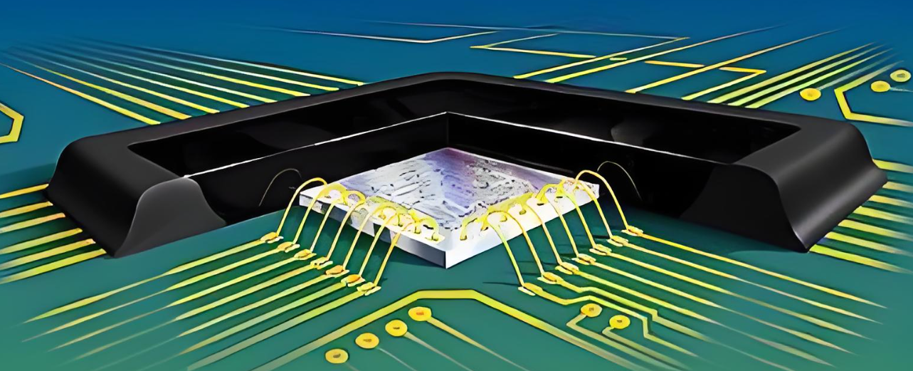
It is especially beneficial in BGA, QFN, CSP, and flip-chip designs where precision and bond strength matter most.
ENEPIG Composition
ENEPIG consists of four distinct layers built on the copper base:
- Copper (Cu) – PCB trace base (not part of the finish, but essential foundation)
- Electroless Nickel (Ni-P) – Acts as a diffusion barrier and solderable layer, typically with 3–10% phosphorus.
- Electroless Palladium (Pd) – Pure palladium layer that prevents nickel corrosion and improves bond reliability.
- Immersion Gold (Au) – Thin, uniform gold for oxidation protection and bond surface preparation.
Each metal in this structure contributes a specific electrical, mechanical, or chemical benefit.
ENEPIG Plating Thickness Specification
The IPC-4556 standard outlines the minimum plating thickness for ENEPIG surface finishes. Here's a common specification chart:
|
Layer |
Typical Thickness Range |
|
Nickel (Ni-P) |
3.0 – 6.0 μm |
|
Palladium (Pd) |
0.05 – 0.15 μm |
|
Gold (Au) |
0.03 – 0.10 μm |
The nickel layer provides a strong base for soldering. The palladium layer ensures a reliable interface for wire bonding, and the thin gold layer preserves the finish during storage.
Electrical Conductivity of ENEPIG
ENEPIG is designed to balance conductivity with durability. While gold and palladium are good conductors, the nickel layer underneath has higher resistance compared to copper or gold. This slight resistance is acceptable in most applications where signal integrity is preserved due to the thinness of the finish.
Conductivity values (approximate):
- Nickel (Ni): 14.3 MS/m
- Palladium (Pd): 9.5 MS/m
- Gold (Au): 45 MS/m
Despite nickel’s lower conductivity, ENEPIG is often preferred for signal lines, especially in high-speed digital and RF boards with fine features.
Thermal Conductivity of ENEPIG
Although ENEPIG's layers are thin, their materials exhibit good thermal properties:
- Nickel: ~90 W/m·K – serves as the main thermal path to the substrate.
- Palladium: ~70 W/m·K – contributes minor heat conduction.
- Gold: ~320 W/m·K – excellent thermal conductor but present in very thin layers.
- Overall Thickness: 3.1–6.3 μm – minimal impact on the overall heat dissipation, which is largely determined by the core material (e.g., metal core or ceramic).
While not as conductive as copper (400 W/m·K), these metals are still suitable for use in thermal management and reflow cycles, especially when the layers are thin and uniformly deposited.
ENEPIG Deposition Process
The ENEPIG deposition process involves a multi-step chemical plating sequence that builds three distinct metal layers—nickel, palladium, and gold—on the exposed copper pads of a PCB. Each step requires strict control of chemistry, temperature, and time to ensure a uniform and defect-free finish.
1. Surface Preparation and Cleaning
The first and most critical step is cleaning the exposed copper pads. Any contaminants, oxides, fingerprints, or organic residues can cause poor adhesion or incomplete plating. The cleaning process typically includes:
- Acid cleaner or alkaline degreasing to remove oils and organics
- Microetching using a mild acid to remove a thin copper layer (usually 1–2 μm), which roughens the surface microscopically
- Pre-dip or activation to prepare the copper for catalytic deposition
2. Electroless Nickel Plating (Ni-P)
After surface prep, the PCB enters an electroless nickel plating bath, which deposits a nickel-phosphorus alloy onto the exposed copper. This is a chemical reduction reaction where nickel ions in solution are reduced and deposited without applying electrical current.
- Nickel Thickness: 3–6 μm (as per IPC-4556)
- Phosphorus Content: Typically 7–10% for high corrosion resistance
- Bath Temperature: 85–90°C
- Reaction Time: ~20–40 minutes, depending on thickness requirement
This nickel layer acts as a barrier to prevent copper diffusion and provides a robust solderable surface for future assembly.
3. Electroless Palladium Plating (Pd)
Once the nickel layer is complete, the board moves to the palladium bath, where a thin layer of palladium is chemically deposited on top of the nickel. This layer also protects the nickel from reacting with the immersion gold solution in the next step, preventing undesired intermetallic compounds.
4. Immersion Gold Plating (Au)
The final step is immersion gold, a displacement reaction where gold ions replace palladium atoms on the surface. This process does not build thick gold layers but deposits a very thin, soft layer of gold just enough to protect the palladium.
5. Final Rinse and Drying
After gold deposition, the PCB is thoroughly rinsed in deionized water to remove any residual plating chemicals. It is then dried using hot air or nitrogen. At this stage, the ENEPIG surface is complete and ready for assembly, storage, or testing.
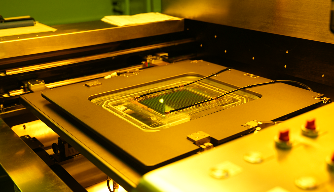
At Best Technology, our plating tanks are automated and monitored in real-time using MES to ensure consistency across batches. We adjust plating times and solution concentrations based on pad size, layout density, and customer specifications. We are the expert in this field.
What Is the IPC Standard for ENEPIG?
ENEPIG surface finishes are regulated by IPC-4556, which sets the quality, performance, and test requirements for electroless palladium and immersion gold over nickel finishes.
The IPC-4556 standard defines:
- Acceptable thickness ranges for Ni, Pd, and Au layers.
- Solderability testing methods (wetting balance, steam aging).
- Wire bond test requirements.
- Visual inspection criteria for surface finish quality.
Manufacturers who follow IPC-4556 ensure consistent and traceable ENEPIG quality across different production batches.
ENIG vs ENEPIG Wire Bonding
While ENIG is widely used, it’s not suitable for wire bonding, especially with gold wire. Here's how they compare:
|
Parameter |
ENIG |
ENEPIG |
|
Structure |
Ni-P + Au |
Ni-P + Pd + Au |
|
Black Pad Risk |
Higher (due to nickel corrosion) |
Lower (Pd protects nickel) |
|
Gold Wire Bonding |
Limited |
Excellent |
|
Aluminum Wire Bonding |
Not supported |
Fully supported |
|
Joint Strength |
Medium |
High |
|
Application Fit |
General-purpose boards |
High-reliability & hybrid packaging |
If your application involves chip-on-board, hybrid modules, or fine-pitch BGA, ENEPIG is the better choice due to its bonding reliability and oxidation resistance.
How Do You Test the ENEPIG Wire Bonding?
Wire bonding reliability on ENEPIG is tested through several methods:
- Ball Pull Test – Measures the force required to break the bond.
- Shear Test – Evaluates bond integrity under lateral stress.
- Visual Inspection – Ensures proper bonding shape and adhesion.
- Aging & Temperature Cycling – Simulates thermal fatigue and oxidation.
- Surface Scanning (SEM/EDS) – Detects cracks, corrosion, or contamination.
At Best Technology, we perform rigorous bond strength testing as part of our in-process quality control, especially for aerospace and medical projects.
Why Choose Best Technology for ENEPIG Surface Finish?
Best Technology offers IPC-4556-compliant ENEPIG plating with tightly controlled processes. Our production lines use MES systems to track every batch, and our engineers fine-tune plating parameters to match your specific product needs.
We support projects in:
- Aerospace
- Medical electronics
- RF modules
- Automotive control systems
- MEMS sensors and gold wire bonding ICs
With certifications like ISO13485, AS9100D, and IATF16949, we serve as a trusted partner for ENEPIG-finished PCBs that must meet critical reliability standards.
FAQs
1. Is ENEPIG suitable for gold wire bonding?
Yes, ENEPIG is ideal for gold and aluminum wire bonding due to its palladium layer.
2. What is the standard ENEPIG plating thickness?
Nickel: 3–6 μm, Palladium: 0.05–0.15 μm, Gold: 0.03–0.10 μm.
3. How does ENEPIG prevent black pad?
The palladium layer acts as a barrier to prevent nickel corrosion, reducing the chance of black pad formation.
4. Is ENEPIG better than ENIG?
For wire bonding and multi-metal compatibility, yes. However, ENIG is more cost-effective for general applications.
5. Is ENEPIG suitable for ceramic PCBs?
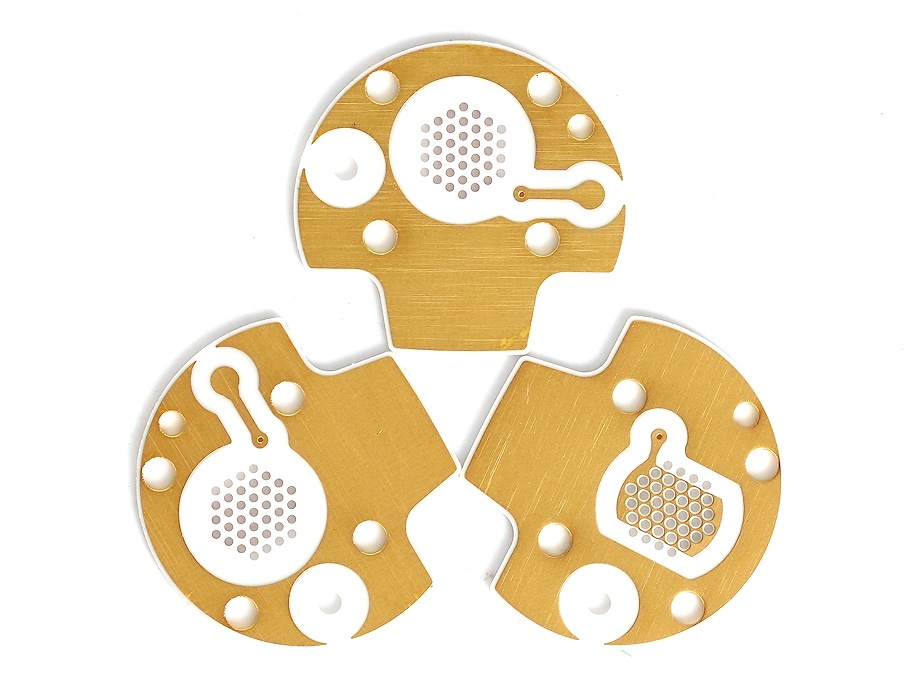
Absolutely. ENEPIG is ideal for ceramic PCBs due to its strong bonding performance, thermal reliability, and surface uniformity.
6. What industries use ENEPIG?
ENEPIG is used in automotive, aerospace, medical, RF, and high-power electronics—anywhere reliability and bonding performance are critical.
 Products
 About us
 Contact us


