


 HOME
HOME

-

Silicon Nitride Substrate, Silicon Nitride Ceramic Substrate Formula
2025 05,08 -
How to choose the appropriate substrate for ceramic circuit boards?
2023 11,16 -
Laser Cutting or Water Saw Cutting? How To Choose the Best Cutting Solution for Ceramic Circuit Boards
2023 11,13 -
Why Ceramic PCB Is So Expensive?
2023 11,10 -
Which Process Ceramic Circuit Board Is A Better Solution For Semiconductor Refrigerator Chips?
2023 11,06 -
Silicon Printing Circuit Boards For Advancing Electronics
2023 10,27 -
What is the Difference Between HTCC and LTCC Ceramic PCB
2023 10,06 -
What is the Difference Between 96% and 99% Aluminum Oxide in Ceramic PCBs?
2023 09,20 -
Why thick film ceramic PCB is good for oil level sensor in automotive industry?
2023 08,25 -
Statistical analysis of ceramic PCB application fields
2023 08,16 -
Notice of anti-static requirements for PCBA processing and production
2023 08,16 -
Silver Paste: The Best Conductor Material for Via Holes in Thick Film Ceramic Boards
2023 08,16 -
Testing Circuit Board Ceramic Diode Fuses: A Complete Guide
2023 08,07 -
Why DBC is replaced by DPC in ceramic PCB manufacturing?
2023 08,01 -
What is thick film ceramic PCB?
2023 08,02
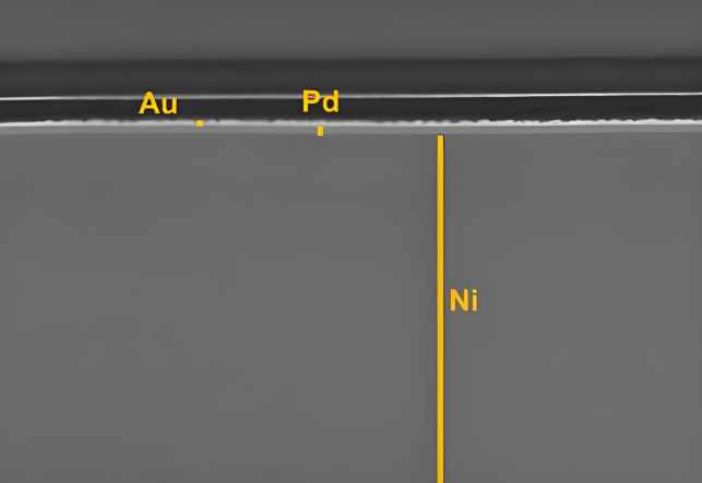
What is the Composition of ENEPIG, Electrical/Thermal Conductivity and Thickness?
ENEPIG stands for Electroless Nickel Electroless Palladium Immersion Gold. It’s a multi-layer surface finish used in PCB manufacturing to enhance solderability, wire bonding, and corrosion resistance. ENEPIG is especially suitable for high-density designs, RF modules, and ceramic-based PCBs due to its support for both gold and aluminum wire bonding, as well as excellent environmental stability. Today, we would like to introduce the composition, plating thickness, and electrical/thermal conductivity of ENEPIG surface finishing.
1. Composition
Copper (Cu) Base: PCB substrate (not part of the ENEPIG layers but serves as the foundation).
Chemical Nickel (Ni-P): Forms a phosphorus-containing nickel layer (typically 3-10% phosphorus) as a diffusion barrier and solderable base 148.
Chemical Palladium (Pd): Pure palladium layer acting as a corrosion inhibitor.
Immersion Gold (Au): Thin gold layer providing oxidation resistance and surface connectivity
2.Layer Thickness Ranges
|
Layer |
Thickness Range |
Key Functions |
|
Nickel (Ni-P) |
3-6 μm (120-240 μinches) |
Barrier against copper diffusion; foundation for soldering. |
|
Palladium (Pd) |
0.05-0.15 μm (2-6 μinches) |
Prevents nickel oxidation ("black pad"); enhances solder joint reliability. |
|
Gold (Au) |
0.03-0.1 μm (1.2-4 μinches) |
Anti-corrosion; ensures surface solderability and wire-bond compatibility. |
3. Electrical Conductivity
Surface Conductivity: Dominated by the gold layer (conductivity: 70 MS/m), enabling low-contact resistance for signals and connectors.
Via/Through-Hole Conductivity: Nickel layer (conductivity: 10-15 MS/m) becomes critical. Its higher resistivity than copper can marginally increase impedance in high-current paths.
High-Frequency Performance: Thin gold (<0.1 μm) minimizes "skin effect" losses, making ENEPIG suitable for RF/microwave PCBs
4. Thermal Conductivity
Nickel Layer: ~90 W/m·K (acts as primary thermal path from components to substrate).
Palladium/Gold: Pd (~70 W/m·K) and Au (~320 W/m·K) contribute minimally due to their thinness.
Overall Impact: ENEPIG’s total thickness (3.1-6.3 μm) has negligible effect on bulk thermal resistance. Heat dissipation is dominated by the PCB substrate (e.g., metal-core PCBs: 160-400 W/m·K)
5. Conclusion
ENEPIG’s multilayer structure balances solderability, corrosion resistance, and electrical performance. Its nickel layer (3-6 μm) provides robustness, palladium (0.05-0.15 μm) prevents failures, and gold (0.03-0.1 μm) ensures surface conductivity. While thermal properties are substrate-dependent, electrical performance excels in high-frequency designs. Recent advances enable thinner layers for 5G/millimeter-wave application
 Products
 About us
 Contact us


