


 HOME
HOME

-

Silicon Nitride Substrate, Silicon Nitride Ceramic Substrate Formula
2025 05,08 -
How to choose the appropriate substrate for ceramic circuit boards?
2023 11,16 -
Laser Cutting or Water Saw Cutting? How To Choose the Best Cutting Solution for Ceramic Circuit Boards
2023 11,13 -
Why Ceramic PCB Is So Expensive?
2023 11,10 -
Which Process Ceramic Circuit Board Is A Better Solution For Semiconductor Refrigerator Chips?
2023 11,06 -
Silicon Printing Circuit Boards For Advancing Electronics
2023 10,27 -
What is the Difference Between HTCC and LTCC Ceramic PCB
2023 10,06 -
What is the Difference Between 96% and 99% Aluminum Oxide in Ceramic PCBs?
2023 09,20 -
Why thick film ceramic PCB is good for oil level sensor in automotive industry?
2023 08,25 -
Statistical analysis of ceramic PCB application fields
2023 08,16 -
Notice of anti-static requirements for PCBA processing and production
2023 08,16 -
Silver Paste: The Best Conductor Material for Via Holes in Thick Film Ceramic Boards
2023 08,16 -
Testing Circuit Board Ceramic Diode Fuses: A Complete Guide
2023 08,07 -
Why DBC is replaced by DPC in ceramic PCB manufacturing?
2023 08,01 -
What is thick film ceramic PCB?
2023 08,02
Best High Thermal Conductivity PCB for NFC Applications
In modern electronics, NFC (Near Field Communication) has become a popular method for secure, short-range wireless communication. However, designers face a unique challenge: building PCBs that not only handle heat effectively but also avoid generating interference that could disrupt NFC performance.
When high power or dense circuits are involved, traditional materials like FR4 or even aluminum PCBs struggle. While aluminum offers good thermal conductivity, it often introduces electromagnetic interference (EMI), which is unacceptable in sensitive communication systems.
So, what’s the solution? The answer lies in high thermal conductivity ceramic PCBs, especially AlN (aluminum nitride) ceramic PCBs, which meet both thermal and EMI requirements for NFC applications.
Why Aluminum PCBs Are Not Suitable for NFC Applications?
Aluminum PCBs are widely used for thermal management in LED lighting, power modules, and automotive applications. But when it comes to NFC, they fall short. The main issue is electromagnetic interference (EMI).
NFC operates at 13.56 MHz, a frequency easily disrupted by nearby conductive metals. Aluminum cores act like antennas or reflectors, which can distort or block signal transmission. Even with good layout practices, the proximity of aluminum can compromise the signal's reliability.
For applications where low noise and high-frequency integrity matter—such as access control, contactless payments, or smart tracking—aluminum is not the right choice.
Importance for High Thermal Conductivity in NFC Devices
NFC may seem like a low-power technology, but in many systems, it coexists with components that generate significant heat. Think of:
- Embedded MCUs
- Wireless charging coils
- Power transceivers
- Sensors with real-time data processing
These modules can overheat if not paired with a PCB that offers strong thermal dissipation, especially in compact, sealed enclosures.
Most engineers target 40 W/mK or above for critical designs. While FR4 or metal-clad PCBs struggle here, ceramic substrates can easily exceed that threshold—particularly aluminum nitride (AlN), which delivers outstanding thermal conductivity without compromising electrical performance.
Why Select Ceramic PCBs as an Alternative?
Ceramic materials have become increasingly popular for thermal-critical applications, thanks to their high conductivity and excellent insulation. The three most common types are:
- Aluminum Nitride (AlN) – 170+ W/mK
- Beryllium Oxide (BeO) – 200–300 W/mK (but toxic)
- Silicon Nitride (Si₃N₄) – 85–95 W/mK
Among these, AlN ceramic PCBs strike the best balance between thermal conductivity, safety, reliability, and manufacturability.
Unlike aluminum, ceramic substrates are non-metallic. They don’t conduct RF energy, which significantly reduces signal distortion and EMI. That makes them ideal for NFC communication systems where signal clarity is critical.
Advantages of AlN Ceramic PCB for NFC Applications
If you’re designing for both thermal efficiency and NFC reliability, AlN ceramic PCBs stand out for several reasons:
- High thermal conductivity (>170 W/mK) enables rapid heat dissipation
- Excellent electrical insulation helps prevent cross-talk and interference
- Low dielectric loss supports high-frequency signals like NFC
- Non-magnetic and non-metallic, minimizing EMI risk
- High strength and reliability under thermal cycling and vibration
In short, AlN ceramic PCB for NFC applications is an optimal solution when your design demands both performance and signal integrity.
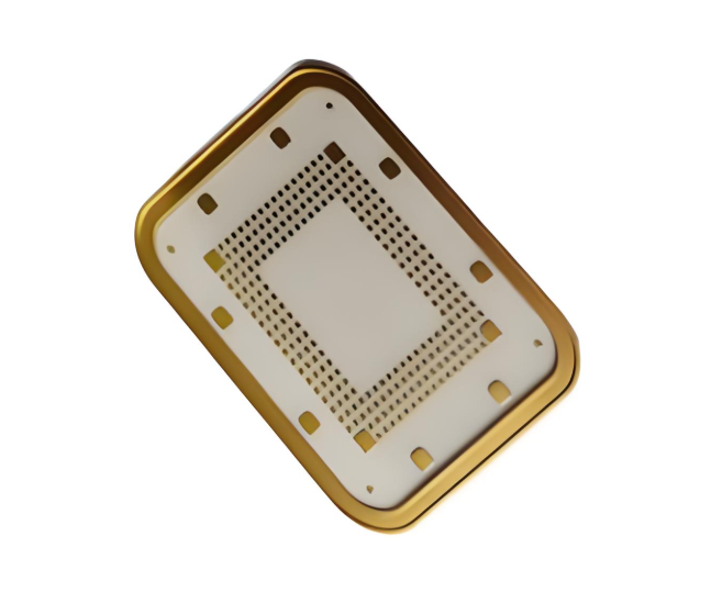
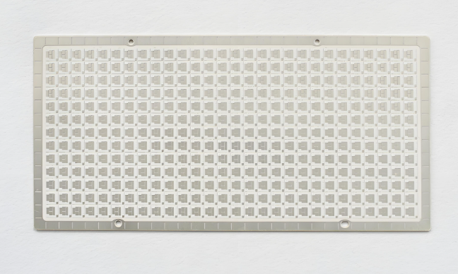
Can AlN Ceramic PCBs Be Manufactured in Large Sizes?
One concern engineers often have is whether ceramic PCBs can be manufactured in large dimensions. The answer is: yes—but with certain limitations and care.
At Best Technology, we can produce AlN ceramic PCBs up to 138mm x 190mm, depending on the design complexity and thickness. However, large-size ceramic boards require:
- Careful sintering to avoid cracks or warping
- Flatness control and proper panel layout
- Precision machining and laser cutting after sintering
For applications like NFC reader arrays, industrial sensors, or RF control modules, ceramic PCB is entirely achievable with the right production partner.
How to Ensure EMI Protection in Ceramic PCB Designs?
Even with AlN as the base, your design layout still plays a vital role in EMI control. Here are tips to further reduce interference:
- Use ground planes to isolate high-frequency circuits
- Keep NFC antenna traces away from noisy power lines
- Place decoupling capacitors close to IC power pins
- Avoid unnecessary vias near sensitive signals
- Shield your enclosure using non-metallic materials with internal copper mesh if needed
By combining low-EMI ceramic substrates with smart layout strategies, your NFC application will be much more robust and reliable.
Best Technology’s Expertise in AlN Ceramic PCB Manufacturing
At Best Technology, we bring unmatched experience and technical capabilities to every AlN ceramic PCB project. With over 19 years of expertise in high-performance ceramic substrates, we’ve supported more than 1,200 customers across industries like aerospace, automotive, medical, and new energy.
Our sales-engineers act as direct technical contacts, helping you avoid the delays of going back and forth between sales and engineering teams. This saves you valuable time during the design and quotation process.
We offer a wide range of ceramic materials, including Aluminum Nitride (AlN), Beryllium Oxide (BeO), and Silicon Nitride (Si₃N₄), to match different thermal and electrical needs.
Best Technology also provides mature ceramic metallization processes such as:
- DBC (Direct Bonded Copper)
- DPC (Direct Plated Copper)
- AMB (Active Metal Brazing)
- Thick film and Thin film technologies
Our integrated manufacturing and quality control systems, combined with full MES traceability, ensure that your AlN ceramic PCBs meet the highest standards for reliability and performance in EMI-sensitive environments like NFC applications.
Common Mistakes When Choosing PCB Material for NFC Devices
Even experienced engineers may fall into these traps:
- Choosing aluminum PCBs for thermal reasons but overlooking EMI effects
- Overestimating FR4’s ability to dissipate heat in small enclosures
- Ignoring the size limitations of ceramic boards until late in the project
- Skipping EMI simulation and testing before mass production
Avoid these mistakes by selecting a material like AlN early in the design process and working with a ceramic PCB specialist.
How to Request a Custom Quote for High Thermal Ceramic PCBs?
Getting a quote is simple. To get started, prepare:
- Gerber files or mechanical drawings
- Layer stack-up details
- Expected power dissipation per module
- Target size (e.g., 138mm x 190mm)
- Required quantity and lead time
Send your requirements to Best Technology, and our engineers will respond within 24 hours. We’ll help you review thermal needs, recommend the best ceramic thickness, and optimize layout for manufacturability.
Conclusion
When your NFC design needs both high thermal performance and zero EMI, aluminum PCBs won’t do the job. AlN ceramic PCBs offer a rare combination of excellent thermal conductivity (over 170 W/mK) and non-metallic, low-noise behavior, making them the best choice for NFC systems.
At Best Technology, we’ve helped dozens of engineers move away from aluminum to ceramic solutions that perform better and last longer. Ready to upgrade your design? Contact us today to discuss your project and get a fast, professional quote.
FAQs
1. What PCB material is best for NFC communication?
Aluminum nitride (AlN) ceramic is the best choice due to its low EMI, high insulation, and strong thermal performance.
2. Can I use ceramic PCBs in high-power NFC applications?
Yes. Ceramic PCBs, especially AlN, can handle high power and maintain reliable NFC performance.
3. Is AlN better than BeO for thermal conductivity?
BeO has higher thermal conductivity but is toxic and more difficult to process. AlN is safer and easier to manufacture.
4. What is the max size of a ceramic PCB available?
At Best Technology, we can produce AlN ceramic PCBs up to 138mm x 190mm depending on thickness and design.
5. How do I minimize EMI in a ceramic PCB design?
Use ground planes, shield high-frequency circuits, and isolate NFC signal paths from power traces.
 Products
 About us
 Contact us


