


 HOME
HOME

-

Ceramic PCB for Humanoid Robot joint actuators
2026 04,07 -
LTCC PCB Surprises: What Most People Miss
2025 12,09 -
Step-by-Step Guide to DPC PCB Design for Sensor Systems
2025 12,03 -
Ceramic PCBs Essential Benefits and Applications
2025 12,01 -
How Al2O3 DPC Ceramic Substrate PCB Enhances Heat Dissipation in Modern Electronics?
2025 11,28 -
How to Choose Between Ceramic, FR4, and Metal Core PCBs
2025 11,27 -
DPC Ceramic PCB Materials: Surprising Science Inside
2025 11,26 -
Wire bondable 2-layer Alumina substrates PCB | Bstceramic PCB
2025 09,22 -
Silicon Nitride Substrate, Silicon Nitride Ceramic Substrate Formula
2025 05,08 -
What is thick film ceramic PCB?
2023 08,02
Automotive AMB Ceramic PCB Fabrication: What Should Customers Know Before Ordering?
Automotive AMB ceramic PCB fabrication is mainly used when standard FR4 PCB, metal core PCB, or even conventional DBC ceramic substrates cannot provide enough thermal cycling strength, insulation reliability, and copper-to-ceramic bonding stability. For customers working on EV inverters, onboard chargers, DC-DC converters, or SiC power modules, the key question is not simply “Can this board dissipate heat?” The real question is whether the substrate can survive repeated heat, current, vibration, and voltage stress over a long automotive service life.
What Is Automotive AMB Ceramic PCB Fabrication?
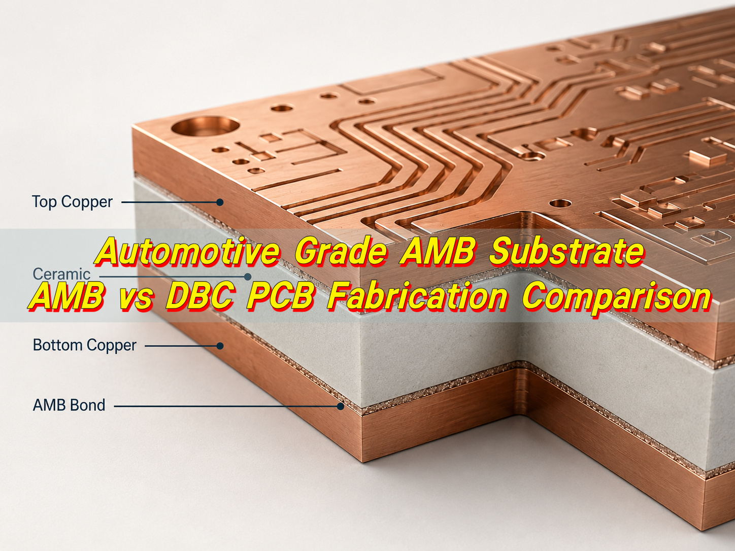
Automotive AMB ceramic PCB fabrication is the manufacturing process of bonding copper directly onto ceramic using active metal brazing, then forming conductive patterns for high-power automotive electronics. AMB stands for Active Metal Brazing. In this process, an active element, commonly titanium in a silver-copper-titanium braze system, helps copper bond strongly to ceramic materials such as silicon nitride or aluminum nitride.
This is different from normal PCB fabrication. FR4 boards use laminated copper foil and glass-reinforced epoxy. Metal core PCBs use a metal base, dielectric layer, and copper circuit. AMB ceramic PCBs use ceramic as the insulating and thermal base, with thick copper bonded to one or both sides.
For customers, AMB fabrication usually matters when the design has one or more of these requirements:
- High current conduction
- High operating voltage
- Strong thermal cycling resistance
- Thick copper requirements
- Compact power module packaging
- SiC or IGBT device mounting
- Long service life in automotive environments
A typical automotive AMB ceramic PCB fabrication flow includes ceramic substrate preparation, copper foil preparation, vacuum brazing, circuit imaging, copper etching, surface finishing, inspection, and reliability testing. The exact route depends on copper thickness, ceramic material, pattern tolerance, surface finish, and whether the substrate will be used as a bare substrate or as part of a larger power module assembly.
In automotive projects, AMB is usually selected for function and reliability, not for low cost. It is best suited for high-value power electronics where substrate failure would cause high replacement cost, module damage, or system-level reliability risk.
What Is an AMB Ceramic Substrate?
An AMB ceramic substrate is a ceramic base with copper bonded to it through an active metal brazing process. The ceramic provides electrical insulation and heat transfer. The copper provides current paths, die-attach areas, wire-bonding areas, and solderable or weldable connection surfaces.
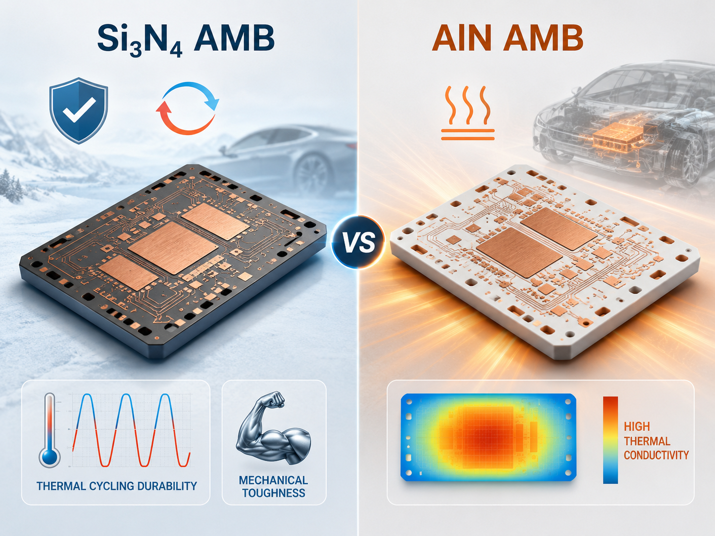
The most common ceramic choices are Si₃N₄ silicon nitride and AlN aluminum nitride. Alumina can also be used in some ceramic PCB designs, but for automotive AMB power modules, Si₃N₄ and AlN are more common because they offer a stronger balance between heat transfer, mechanical strength, and electrical insulation.
The decision logic is simple: choose AlN when thermal conductivity is the dominant requirement; choose Si₃N₄ when thermal cycling, mechanical strength, and reliability under repeated stress are more important.
| Material | Main Advantage | Typical Use Case | Practical Limitation |
|---|---|---|---|
| Si₃N₄ AMB ceramic substrate | High fracture toughness and strong thermal cycling resistance | EV inverters, SiC power modules, traction modules, harsh automotive electronics | Thermal conductivity is usually lower than high-grade AlN |
| AlN AMB ceramic substrate | High thermal conductivity | High heat-flux modules, compact power devices, laser or power electronics | More brittle than Si₃N₄ under severe thermal-mechanical stress |
| Al₂O₃ ceramic substrate | Lower cost and mature supply | Medium-power circuits, less severe thermal cycling conditions | Lower thermal conductivity and lower mechanical robustness than Si₃N₄ for demanding EV modules |
For EV power modules, copper thickness is also part of the substrate decision. Some commercial Si₃N₄ AMB substrates support copper thicknesses from about 0.30 mm to 0.80 mm, which is much thicker than conventional PCB copper and suitable for high-current power paths.
Why Is AMB Ceramic Used in Automotive Electronics?
AMB ceramic is used in automotive electronics because it solves three problems at the same time: heat transfer, insulation, and copper bonding reliability. Automotive power electronics face repeated heating and cooling. When copper, ceramic, solder, semiconductor dies, and baseplates expand at different rates, stress builds at material interfaces. Weak bonding or brittle substrates can crack, delaminate, or lose electrical performance.
AMB is especially valuable in EV and hybrid vehicle systems because current density is rising while module size is shrinking. SiC MOSFETs and advanced IGBT modules can switch higher voltages and operate at higher junction temperatures than older devices. This pushes more thermal and mechanical stress into the substrate.
AMB is usually worth considering when the design includes:
- SiC MOSFET or IGBT power modules
- EV traction inverters
- Onboard chargers
- DC-DC converters
- Battery energy conversion units
- High-voltage power distribution modules
- High-current busbar-linked ceramic substrates
- Compact modules with limited cooling area
It is usually unnecessary for low-power signal circuits, standard control boards, infotainment boards, LED indicator boards, or sensor PCBs that can be handled by FR4, high-Tg FR4, IMS, or conventional ceramic PCB solutions.
For automotive quality planning, customers should also understand that AMB substrate selection is only one part of the qualification chain. IATF 16949:2016 defines automotive quality management system requirements, while standards such as IPC-6012 automotive addenda, AEC-Q series tests, and IPC-9701B may be referenced depending on the product type and assembly reliability scope.
How Does AMB Ceramic Work in EV Power Modules?
In an EV power module, the AMB ceramic substrate sits between the semiconductor devices and the cooling structure. The upper copper layer carries current and provides die-attach pads. The ceramic layer provides electrical insulation while allowing heat to move downward. The bottom copper layer improves heat spreading and provides a bonding surface to a baseplate or cooler.
A simplified stack may look like this:
| Layer | Function in EV Power Module |
| Power semiconductor die | Performs switching or rectification, often SiC MOSFET, diode, or IGBT |
| Die attach layer | Bonds die to copper and transfers heat |
| Top copper circuit | Carries current and forms die, wire bond, or clip-bond areas |
| Ceramic layer | Provides insulation and thermal transfer |
| Bottom copper layer | Spreads heat and supports baseplate attachment |
| Baseplate or cooler | Moves heat into the cooling system |
The reason AMB works well in EV modules is the interface strength between copper and ceramic. In power cycling, the copper expands more than ceramic. If the copper-ceramic bond is weak, the interface becomes a fatigue point. AMB improves this interface by forming a strong metallurgical bond during vacuum brazing.
The practical benefit is not only lower thermal resistance. It is also better survival under repeated thermal cycling. Studies on AMB substrates for SiC power modules have examined temperature cycling from -40°C to 250°C, showing why tough ceramic systems are important for high-temperature module reliability.
For customers, the module layout should be reviewed together with the AMB substrate design. Die position, copper island size, copper symmetry, ceramic thickness, and cooling method all affect stress distribution. A layout that looks electrically correct may still create local stress concentration during power cycling.
Best ceramic PCB fabrication method for high voltage EV?
For high-voltage EV power modules, AMB is often the best ceramic PCB fabrication method when the design requires thick copper, strong bonding, high insulation, and severe thermal cycling performance. DBC is still widely used and cost-effective in many power modules, but AMB becomes more attractive as voltage, temperature swing, and mechanical stress increase.
The choice should be based on the actual stress profile, not only on voltage rating.
| Fabrication Method | Suitable For | Strength | Limitation |
| DBC ceramic substrate | Mature power modules, many IGBT applications, cost-sensitive designs | Good thermal path and mature process | Lower thermal cycling robustness than Si₃N₄ AMB in demanding conditions |
| AMB ceramic substrate | EV inverters, SiC modules, high-current and high-reliability modules | Strong copper-ceramic bonding and strong thermal cycling capability | Higher cost and tighter process control requirements |
| DPC ceramic PCB | Fine circuits, LED, sensors, RF, lower copper thickness designs | Good fine-line capability | Not ideal for heavy copper EV power module paths |
| Thick film ceramic PCB | Resistor networks, heaters, sensors, hybrid circuits | Flexible material system | Limited current capacity compared with thick copper AMB |
| IMS / metal core PCB | LED, power supply, medium-power thermal boards | Cost-effective heat spreading | Organic dielectric limits high-temperature and high-voltage module reliability |
For high-voltage EV use, AMB is not automatically required for every power board. It is most justified when the substrate must combine high current, high voltage insulation, thick copper, and long thermal cycling life in a compact package.
Customers should provide working voltage, peak voltage, isolation requirement, creepage and clearance target, copper thickness, ceramic thickness, device type, expected thermal cycling range, and cooling method before asking for a quotation. Without these details, the supplier can only estimate the substrate, not optimize it.
Why use si3n4 AMB PCB in silicon carbide modules?
Si₃N₄ AMB PCB is widely considered a strong match for silicon carbide modules because SiC devices create a demanding combination of high temperature, fast switching, high power density, and repeated thermal cycling. The substrate must not only move heat. It must also resist cracking and copper delamination.
SiC modules often run at higher temperature swings than traditional silicon-based modules. That means the ceramic must tolerate repeated mechanical stress from copper expansion. Si₃N₄ has higher fracture toughness than many other ceramic materials, so it performs well where thermal cycling is a major reliability driver.
| Requirement in SiC Module | Why Si₃N₄ AMB Helps |
| High thermal cycling stress | Si₃N₄ offers strong fracture toughness and bending strength |
| Thick copper layout | AMB bonding supports robust copper-ceramic adhesion |
| Compact module size | Higher mechanical strength allows thinner ceramic options in some designs |
| High power density | Good heat transfer with improved mechanical durability |
| Automotive reliability target | Better resistance to crack propagation under repeated temperature changes |
Si₃N₄ does not always beat AlN in raw thermal conductivity. Its advantage is the balance between thermal performance and mechanical reliability. Research and supplier data consistently position Si₃N₄ AMB as a preferred option for demanding power electronics where thermal cycling is severe.
For purchasing decisions, Si₃N₄ AMB is usually a practical choice when the project involves SiC inverters, traction modules, high-current switching, or a long vehicle lifetime target. If the design is mainly heat-flux limited but has moderate mechanical cycling stress, AlN AMB may still be competitive.
What Automotive PCB Components Use AMB Ceramic Substrates?
AMB ceramic substrates are not used across all automotive PCB components. They are mainly used in power conversion and power distribution areas where high voltage, high current, and thermal cycling are concentrated.
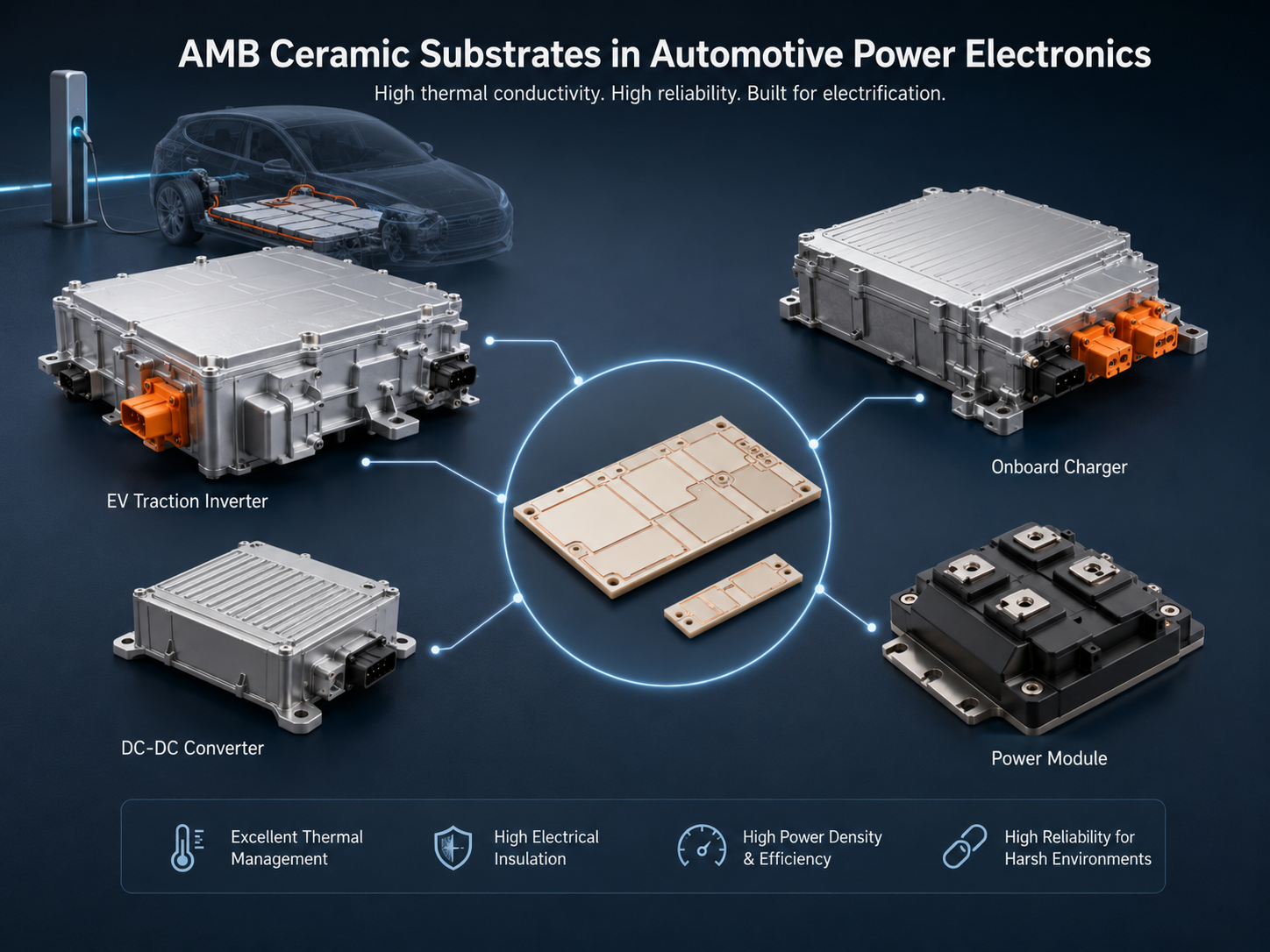
Common automotive applications include:
- EV traction inverter power modules
- SiC MOSFET modules
- IGBT power modules
- Onboard charger power stages
- DC-DC converter modules
- Battery management power interfaces
- High-voltage compressor drive modules
- Electric power steering power modules
- PTC heater power control modules
- High-current ceramic-based power interconnects
AMB ceramic is usually unnecessary for low-current automotive control boards, CAN/LIN communication boards, display control PCBs, infotainment electronics, simple lighting control PCBs, or standard sensor interface boards. These products often use FR4, high-Tg FR4, HDI PCB, flexible PCB, or aluminum PCB depending on design needs.
For a customer evaluating automotive PCB components, the main purchasing question is: Is the ceramic substrate part of the power path or only part of the control circuit? If it is part of the power path, AMB may be relevant. If it only carries signals, logic, or low-current control, AMB will usually add cost without improving product value.
Why Is Copper Bonding Important in AMB Ceramic PCB Fabrication?
Copper bonding is one of the most important quality factors in AMB ceramic PCB fabrication because the copper-ceramic interface carries both electrical and mechanical load. Thick copper expands and contracts during thermal cycling. If the bond is weak or uneven, cracks can start at the interface, especially near copper edges, corners, and large copper islands.
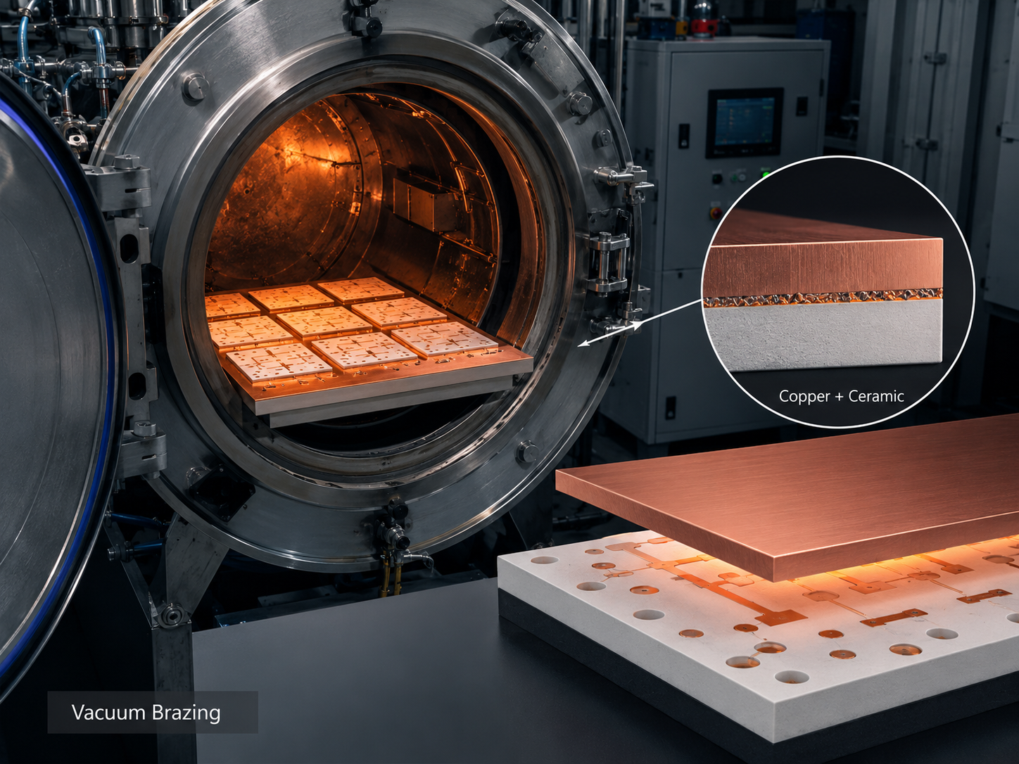
In AMB fabrication, copper is bonded to ceramic in a vacuum brazing process. The active metal in the braze alloy reacts with the ceramic surface and helps create a strong bond. After brazing, the copper is patterned by etching to form circuits, pads, and current paths.
Key copper bonding factors include:
- Copper thickness on top and bottom sides
- Copper symmetry between both sides
- Braze alloy system
- Vacuum brazing temperature control
- Copper edge shape and corner radius
- Ceramic surface condition
- Void control at the bonding interface
- Peel strength and post-cycling adhesion
- Surface finish compatibility with die attach or soldering
Heavy copper AMB ceramic PCB manufacturing requires more careful stress control than thin copper ceramic PCB fabrication. Thick copper improves current capacity and heat spreading, but it also increases mechanical stress during thermal cycling. This is why substrate design should avoid unnecessary sharp corners, extreme copper imbalance, and large unsupported copper areas.
A supplier should be able to discuss copper thickness, minimum etching gap, edge compensation, peel strength testing, plating options, and inspection methods. If the project is for automotive power modules, copper bonding quality is not a cosmetic issue. It is a core reliability parameter.
What Design Factors Affect AMB Ceramic PCB Performance?
AMB ceramic PCB performance is determined by the full stack design, not just ceramic material. Customers should review electrical, thermal, mechanical, and manufacturing limits before freezing the drawing.
| Design Factor | Why It Matters | Customer Decision Logic |
| Ceramic material | Controls thermal conductivity, strength, and fracture toughness | Use Si₃N₄ for severe thermal cycling; consider AlN for higher thermal conductivity |
| Ceramic thickness | Affects insulation, thermal resistance, and mechanical strength | Thinner ceramic improves heat flow but may reduce voltage margin and handling strength |
| Copper thickness | Affects current capacity and heat spreading | Use thick copper only where current and thermal spreading justify the added stress |
| Copper balance | Reduces warpage and thermal stress | Keep top and bottom copper reasonably balanced where possible |
| Copper pattern geometry | Affects etching accuracy and crack risk | Avoid sharp corners and narrow stress concentration zones |
| Creepage and clearance | Supports high-voltage safety | Define working voltage, peak voltage, pollution degree, and system insulation requirement |
| Surface finish | Affects soldering, die attach, wire bonding, and storage | Select finish based on assembly process, not appearance |
| Via or laser drilling requirement | Affects cost and tolerance | Confirm if holes are functional, mounting-related, or only alignment features |
| Substrate outline tolerance | Affects module assembly | Match tolerance to housing, baseplate, and bonding process |
| Thermal cycling requirement | Determines reliability test plan | Define cycle range, dwell time, and acceptance criteria early |
AMB ceramic PCB laser drilling tolerances depend on ceramic type, thickness, hole diameter, and edge distance. For quotation, customers should specify hole function clearly. A mounting hole, alignment hole, laser via, and metallized through feature have different process risks and inspection needs.
For EV inverter substrates, design review should pay special attention to copper edge-to-ceramic edge distance, copper island spacing, die pad flatness, solder void sensitivity, and baseplate attachment method. These details influence manufacturing yield and field reliability more than small changes in nominal thermal conductivity.
How to choose AMB ceramic PCB manufacturer for automotive?
Choosing an AMB ceramic PCB manufacturer for automotive projects should be based on process capability, engineering communication, traceability, and reliability support. Price is important, but the cheapest substrate can become expensive if it causes module redesign, assembly yield loss, or delayed qualification.
A practical supplier evaluation should cover the following points:
| Evaluation Item | What to Check |
| Material capability | Si₃N₄, AlN, copper thickness range, ceramic thickness range, available panel size |
| Process capability | Vacuum brazing control, copper etching accuracy, surface finish options, substrate flatness control |
| Automotive support | Traceability, inspection records, PPAP-related communication, batch consistency, change control |
| Reliability support | Thermal cycling, peel strength, insulation resistance, dielectric withstand, metallographic inspection |
| Design review | Copper balance, corner radius, creepage, clearance, stress zones, manufacturability limits |
| Prototype service | Small-batch trial, drawing review, material suggestion, quotation feedback, lead-time clarity |
| Assembly understanding | Die attach, soldering, wire bonding, clip bonding, baseplate attachment, cleaning compatibility |
For automotive certification standards for AMB ceramic PCB projects, customers should avoid a common misunderstanding: a bare AMB substrate is usually not “AEC-qualified” by itself in the same way as a packaged semiconductor component. Instead, the complete product, module, or assembly may need to satisfy customer-specific reliability and quality requirements. IATF 16949 supports automotive quality management, IPC automotive addenda support PCB performance requirements, and AEC-Q series documents apply to specific automotive electronic component categories.
Before requesting a quotation, prepare the following information:
- Ceramic material: Si₃N₄, AlN, or open to recommendation
- Ceramic thickness
- Copper thickness on each side
- Finished substrate size and quantity
- Circuit drawing, Gerber, DXF, or mechanical drawing
- Surface finish requirement
- Voltage and insulation requirement
- Current load and thermal load
- Operating temperature and thermal cycling target
- Die attach, soldering, wire bonding, or clip bonding process
- Required inspection or reliability test items
- Prototype quantity and mass production estimate
BSTCeramicPCB can support customers who need engineering communication before ordering, especially when the project involves custom AMB ceramic PCB manufacturing for EV power modules, SiC inverter substrates, heavy copper ceramic layouts, or automotive-grade ceramic PCB rapid prototyping. The most useful first step is to send the drawing, stack requirement, electrical load, thermal condition, and expected application, so the fabrication team can review whether AMB is the correct solution or whether another ceramic PCB structure would be more practical.
Conclusion
Automotive AMB ceramic PCB fabrication is suitable for high-power automotive electronics where thermal cycling, copper bonding strength, electrical insulation, and compact module packaging are all critical. It is especially useful for EV inverters, SiC power modules, onboard chargers, DC-DC converters, and other high-current systems.
The best purchasing decision starts with clear application data. Customers should not choose AMB only because it sounds advanced. They should choose it when the electrical, thermal, and reliability demands justify its cost. If you are evaluating an AMB ceramic substrate or need help reviewing a design for manufacturability, contact BSTCeramicPCB at sales@bstceramicpcb.com with your drawings, stack requirements, quantity, voltage, current, and thermal cycling conditions.
 Products
 About us
 Contact us


