






















































 HOME


-

Ceramic PCB for Humanoid Robot joint actuators
2026 04,07 -
LTCC PCB Surprises: What Most People Miss
2025 12,09 -
Step-by-Step Guide to DPC PCB Design for Sensor Systems
2025 12,03 -
Ceramic PCBs Essential Benefits and Applications
2025 12,01 -
How Al2O3 DPC Ceramic Substrate PCB Enhances Heat Dissipation in Modern Electronics?
2025 11,28 -
How to Choose Between Ceramic, FR4, and Metal Core PCBs
2025 11,27 -
DPC Ceramic PCB Materials: Surprising Science Inside
2025 11,26 -
Wire bondable 2-layer Alumina substrates PCB | Bstceramic PCB
2025 09,22 -
Silicon Nitride Substrate, Silicon Nitride Ceramic Substrate Formula
2025 05,08 -
What is thick film ceramic PCB?
2023 08,02
What Should You Specify for a 4mm x 4mm Ceramic Substrate?
Published:
A 4mm x 4mm ceramic substrate is a finished electronic substrate with a nominal 4 mm by 4 mm outline. It is not a 4 inch square ceramic sheet and it is not 4 mm ceramic tumbling media. At this scale, material, thickness, edge clearance, metallization, panel layout and inspection method must be defined together because a small change can consume a meaningful part of the usable circuit area.
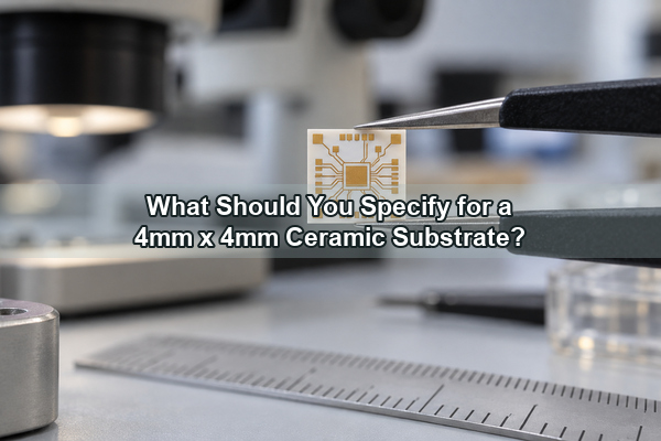
What Does a 4mm x 4mm Ceramic Substrate Mean?
The 4 mm by 4 mm dimension normally describes the finished length and width. It does not define substrate thickness, ceramic grade, conductor system, corner radius, surface finish or dimensional tolerance. Those items belong in the drawing and purchase specification.
The drawing should also state whether 4.00 mm is the target value or only a nominal description. A part called 4 mm square can still require a bilateral tolerance, a profile tolerance, or inspection against a customer-supplied CAD file. For a ceramic circuit, the finished outline must be interpreted together with edge metallization clearance, conductor registration and the chosen singulation method.
How Much Circuit Area Is Actually Available?
The usable circuit area is smaller than 16 mm2. Copper or thick-film conductors cannot normally extend to every edge without considering chipping, electrical clearance, plating behavior and handling. Fiducials, wire-bond pads, solder pads, vias, resistor elements and component keep-outs further reduce the space available for routing.
A practical layout starts from the edge inward. First reserve the approved edge clearance and corner geometry. Then place the largest functional pads, high-current paths and thermal interfaces. Only after these constraints are fixed should fine signal routing fill the remaining area. Supplying a dimensioned CAD file is much safer than asking a manufacturer to scale an image into a 4 mm square.
Which Ceramic Material Fits the Design?
Material selection should follow the electrical, thermal and mechanical problem, not the white or gray appearance of a sample.
| Material | When it is commonly considered | Main design question |
|---|---|---|
| 96% alumina (Al2O3) | General insulation, stable ceramic circuitry and cost-sensitive designs | Is its thermal path sufficient for the heat load? |
| Aluminum nitride (AlN) | Higher heat-flow requirements with electrical insulation | Are the metallization, handling and cost targets compatible? |
| Silicon nitride (Si3N4) | Thermal cycling or mechanical-reliability demands | Does the application justify its material and process requirements? |
For a small alumina design, our small DPC ceramic substrate for compact sensor circuits shows why conductor density and pad placement matter as much as the bulk ceramic property. We review Al2O3, AlN and Si3N4 as different engineering systems; one material is not a drop-in replacement for another.
Which Thickness Should You Specify?
Thickness affects stiffness, thermal resistance, laser processing, handling and the overall package height. A thinner ceramic can shorten the through-thickness heat path and reduce profile, but it is also more sensitive to handling and assembly support. A thicker ceramic is easier to handle in some processes but adds thermal path length and may not suit a low-profile package.
For DPC projects, we review substrate thicknesses within our published 0.15-6.0 mm reference range, but this is not a promise that every thickness, material and 4 mm outline can be combined. The final choice depends on ceramic grade, metallization stack, via structure, panel method and required flatness. The purchase specification should therefore identify both the nominal thickness and its tolerance.
Which Metallization Process Fits a 4mm Footprint?
The circuit geometry and copper requirement usually decide the process. DPC is suitable when a small substrate needs fine conductors, compact pads or plated features. Thick film is useful for screen-printed conductors, resistors and hybrid-circuit functions. Thin film supports very fine, controlled metallization for specialized circuits. DBC uses bonded copper for higher-current and thermal applications, but its thicker copper and coarser geometry must be evaluated against the limited 4 mm footprint.
Our tiny custom DBC ceramic substrate is relevant when current capacity and robust copper are more important than very fine routing. Our thin film ceramic PCB is the more relevant reference when the design priority is controlled fine-feature metallization. The choice should come from the actual conductor thickness, minimum feature, current and assembly method rather than from substrate size alone.
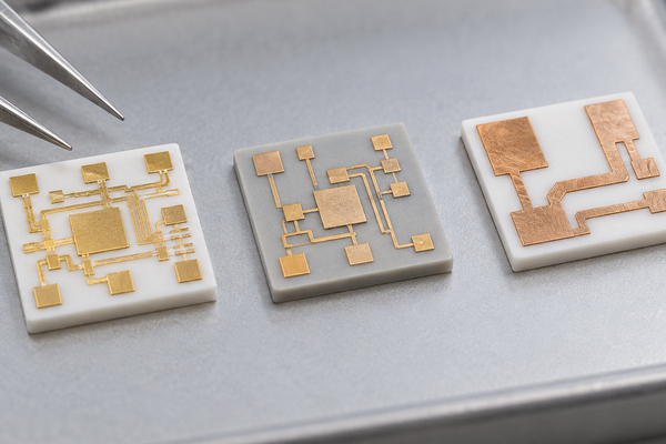
How Should Pads, Traces and Vias Be Laid Out?
On a 4 mm square, routing margins disappear quickly. The layout should define minimum line width and spacing, pad size, conductor-to-edge clearance, via diameter, via-to-pad relationship and registration tolerance. If wire bonding is required, pad finish, bond direction, loop clearance and probe access must be considered before routing is frozen.
Our published DPC reference capability includes 0.075/0.075 mm minimum line/space and a 100 micrometer minimum hole diameter. These values are capability references, not automatic design rules. A production review must still consider copper thickness, aspect ratio, material, yield, electrical isolation and the inspection method. Designing every feature at a published minimum leaves no margin for process interaction.
How Do Thermal and Electrical Requirements Interact?
A small ceramic substrate can move heat only if the complete path is designed. The heat source, die attach or solder layer, metallization area, ceramic thickness, interface material and heat sink all contribute to junction-to-ambient performance. A high-conductivity ceramic cannot compensate for a small thermal pad or a poor external interface.
Electrical isolation must be reviewed at the same time. Higher voltage may require larger creepage and clearance distances, which directly compete with routing area. High current may require thicker or wider conductors, while RF or precision circuits may prioritize controlled geometry and dielectric behavior. The drawing should identify operating voltage, current, power, frequency and temperature rather than asking the material name to carry all design requirements.
Why Do Edge Clearance, Corner Radius and Chipping Matter?
Ceramic is hard but brittle. Edge chips, sharp internal corners and stress concentrations can affect handling, assembly and long-term reliability. On a 4 mm part, even a small chip can approach a conductor or reduce the mechanical support under a pad.
Define the acceptable edge-chip limit, corner condition and conductor-to-edge distance on the drawing. Also state whether dimensions are measured over the ceramic only or over any edge metallization. Our published laser-outline reference tolerance is +/-0.13 mm for selected ceramic PCB processes; a tighter 4 mm outline requires a project-specific review of material, thickness, profile and inspection method.
Should the Parts Be Supplied Individually or in a Panel?
Loose 4 mm squares are difficult to handle, print, inspect and assemble in volume. A process panel can improve orientation, traceability and automated handling. It can also provide tooling holes, fiducials, coupons and a protected border around the active parts.
Panel design is not simply an array calculation. The rail width, pitch, breakaway structure, laser streets, tooling references and assembly equipment all affect the delivered format. If the customer needs individual parts, we can still evaluate whether manufacturing and testing should occur in a panel before final separation.
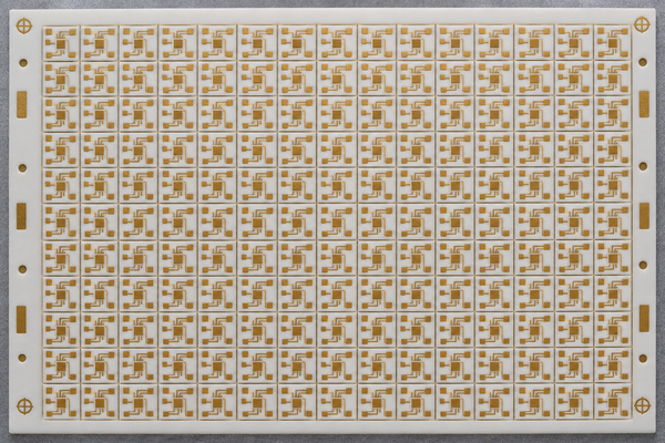
How Are 4mm x 4mm Ceramic Substrates Singulated?
Laser cutting, laser scribing and mechanical separation can produce different edge conditions. The appropriate route depends on substrate material, thickness, dimensional tolerance, edge quality, panel configuration and cost target.
A fully laser-cut outline supports custom profiles but needs an approved kerf and heat-affected-zone review. Scribed arrays can be efficient for regular rectangular parts, but the residual web and break direction influence edge quality. The manufacturing drawing should show whether the final 4 mm dimension is measured after separation and whether burrs, taper, recast or chips have specific limits.
Which Surface Finish Supports the Assembly Process?
Surface finish must match the next assembly operation. ENIG may suit soldering and selected wire-bond requirements when the complete stack is approved. Electroplated nickel/gold can be selected for particular contact or bonding needs. Immersion silver, OSP and other finishes have different storage, handling and assembly implications.
Do not specify a finish only by name. State whether the pads will be soldered, wire bonded, probed, adhesively attached or used as contacts. If wire bonding is required, include wire material, bond method and pad acceptance criteria. Finish thickness and nickel condition should be treated as controlled manufacturing inputs, not assumed from a generic finish label.
What Should a Prototype and Inspection Plan Verify?
A useful prototype verifies more than whether one sample powers on. It should confirm finished dimensions, thickness, flatness where relevant, conductor registration, line/space, via continuity, isolation, surface finish, pad geometry and edge quality. Thermal or cycling tests should reflect the actual assembly if those stresses drive the design.
For very small parts, the inspection fixture and datum strategy matter. Optical measurement must identify the ceramic edge clearly, and electrical probes must contact pads without damaging the finish. Lot traceability, panel position and coupon data can help separate a layout issue from a material or process issue.
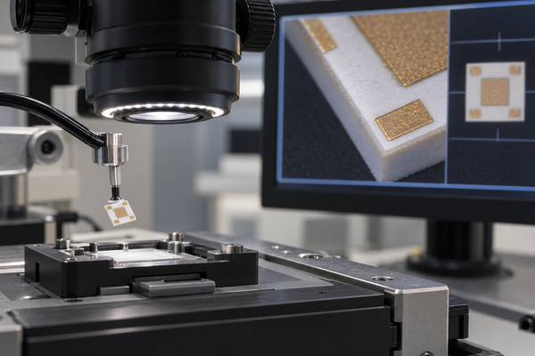
What Applications Use a 4mm x 4mm Ceramic Substrate?
This footprint can suit compact sensor circuits, LED or laser-diode submounts, miniature hybrid circuits, RF modules, medical sensing assemblies and localized power-device interfaces. The substrate does not perform these functions by size alone. Each application needs a matching metallization, thermal path, pad arrangement, assembly method and qualification plan.
For an LED submount, the critical inputs may be die pad geometry, heat spreading and attachment. For a sensor circuit, fine routing, stable insulation and compact interconnection may dominate. For an RF element, conductor geometry and frequency-dependent material data become more important. The same 4 mm outline can therefore require very different manufacturing routes.
What Information Should Be Included in the RFQ?
To quote and review a 4 mm square ceramic circuit without guessing, send us:
- Gerber, ODB++, DXF or another dimensioned circuit file;
- ceramic material, grade, finished thickness and tolerances;
- finished 4.00 mm x 4.00 mm outline, corner and edge requirements;
- metallization process, conductor thickness and minimum features;
- via, cavity, wraparound or edge-metallization requirements;
- surface finish and the intended soldering, bonding or contact method;
- operating voltage, current, power, frequency and temperature;
- individual-part or panel-delivery requirements;
- prototype quantity, production quantity and inspection criteria.
We use these inputs to review process fit, panel strategy, inspection access and the main manufacturing risks before quotation. Email the drawing and specification to sales@bstceramicpcb.com. If some items are not yet fixed, identify them as open design decisions instead of assigning an unsupported tolerance.
A 4mm x 4mm ceramic substrate is manufacturable only when its small outline is connected to a complete material, metallization, layout, separation and inspection specification. That engineering definition is what turns a nominal size into a repeatable ceramic circuit.
 Products
 About us
 Contact us



