






















































 HOME
HOME

-

Ceramic PCB for Humanoid Robot joint actuators
2026 04,07 -
LTCC PCB Surprises: What Most People Miss
2025 12,09 -
Step-by-Step Guide to DPC PCB Design for Sensor Systems
2025 12,03 -
Ceramic PCBs Essential Benefits and Applications
2025 12,01 -
How Al2O3 DPC Ceramic Substrate PCB Enhances Heat Dissipation in Modern Electronics?
2025 11,28 -
How to Choose Between Ceramic, FR4, and Metal Core PCBs
2025 11,27 -
DPC Ceramic PCB Materials: Surprising Science Inside
2025 11,26 -
Wire bondable 2-layer Alumina substrates PCB | Bstceramic PCB
2025 09,22 -
Silicon Nitride Substrate, Silicon Nitride Ceramic Substrate Formula
2025 05,08 -
What is thick film ceramic PCB?
2023 08,02
AIN Ceramic PCB Manufacturing Services: From DFM to Production
AIN ceramic PCB manufacturing services turn an aluminum nitride substrate into a manufacturable circuit by matching the ceramic grade, metallization process, copper geometry, surface finish and inspection plan to the application. The service is most useful when a compact power, LED, laser or RF assembly needs substantially better heat transfer than alumina while retaining electrical insulation.
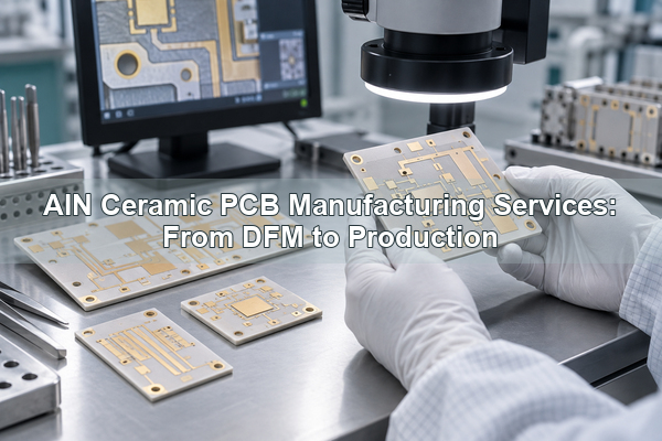
The correct chemical symbol is AlN, with a lowercase “l,” although “AIN ceramic PCB” is also used in searches and purchasing communication. At BSTCeramicPCB, we review the drawing and assembly requirements before selecting DPC, DBC, AMB, thick-film or thin-film processing. This prevents a material choice from being separated from the copper structure and joining process that determine actual production performance.
What Do AIN Ceramic PCB Manufacturing Services Include?
The scope can start with a bare AlN substrate or a completed circuit drawing. A complete manufacturing service should connect five decisions: substrate grade, metallization route, circuit pattern, assembly surface and verification method.
Typical deliverables include:
- DFM review of substrate thickness, outline, holes, copper-to-edge distance and tolerances;
- selection of DPC, DBC, AMB, thick-film or thin-film processing;
- conductor patterning, via metallization and compatible surface finishing;
- dimensional, visual, electrical and process-specific inspection;
- prototype feedback before repeat or volume production.
Assembly may be a separate scope. The inquiry should state whether the supplier is quoting bare ceramic circuits, die attach, wire bonding, soldered components or a complete module.
When Is an AlN Ceramic PCB the Right Choice?
AlN is justified when the substrate itself is a meaningful part of the thermal path. Commercial grades commonly provide far higher thermal conductivity than alumina while remaining electrically insulating, and their coefficient of thermal expansion is relatively close to silicon. These properties suit compact circuits with high local heat flux or bare-die attachment.
AlN is often unnecessary when heat generation is modest, board area is generous or an alumina design already meets the junction-temperature target. The material also costs more and is brittle. A useful selection check is to model the complete heat path, including die attach, copper, ceramic, baseplate and interface material, rather than comparing ceramic conductivity alone.
Which AlN PCB Manufacturing Process Fits the Design?
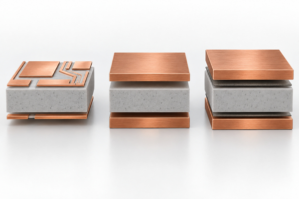
Choose the process by conductor thickness, feature size, current and reliability requirements. The same AlN material can support very different circuit constructions.
| Process | Conductor Structure | Best Fit | Main Design Trade-off |
|---|---|---|---|
| DPC | Seed layer plus plated copper | Fine-to-medium features, patterned vias and controlled copper build | Plating distribution and seed removal |
| DBC | Thick copper bonded to AlN | High-current power modules and strong lateral heat spreading | Etch allowance, stress and copper-to-ceramic thickness balance |
| AMB | Copper brazed to ceramic with an active interface | Power modules requiring robust copper-ceramic attachment | Braze system, residual stress and process qualification |
| Thick film | Printed and fired conductor paste | Hybrid circuits, resistors and practical patterned conductors | Fired geometry and paste compatibility |
| Thin film | Deposited and patterned metal stack | Fine-pitch, RF, photonic and wire-bonding structures | Surface quality, metal-stack control and cost |
Our double-sided aluminum nitride DPC ceramic circuit is a relevant construction when the design needs patterned conductors on both sides. A high-current module may instead require a thick-copper DBC or AMB structure.
How Should the AlN Substrate Grade Be Specified?
Do not specify only “aluminum nitride.” State the required thermal-conductivity grade, thickness, length and width, surface condition, flatness or warpage limit, and any edge or hole quality requirements. Thermal conductivity is grade-dependent; a generic datasheet value should not be treated as the guaranteed value for every production lot.
For die attach or thin-film circuitry, surface roughness and local flatness may affect bond-line control and pattern continuity. For a DBC power substrate, ceramic thickness must be evaluated together with copper thickness and isolation voltage. If the design uses laser-cut outlines or holes, define finished dimensions and allowable chipping at functionally critical edges.
Copper Thickness, Line Geometry and Via Requirements
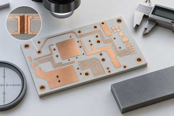
The drawing should specify finished copper thickness rather than only artwork or plating time. Conductor width, spacing and etch compensation depend on that thickness: a layout that is practical with thin plated copper may not transfer directly to thick DBC copper.
For each hole, identify whether it is unplated, wall-plated, filled or intended only for mechanical alignment. Ceramic thickness, hole diameter and taper influence metallization continuity. If a via carries current or forms an RF ground path, specify the required electrical result and test method instead of relying on nominal hole size alone.
Keep copper features away from cut edges and stress concentrations. Final values should be confirmed against the selected process, copper thickness and substrate thickness; using one universal ceramic PCB design rule can create unnecessary cost or an unmanufacturable layout.
Surface Finish, Planarity and Die-Attach Requirements
Surface finish must match the next assembly operation. Soldering, gold wire bonding, aluminum wire bonding, sintered-silver die attach and brazing impose different requirements on the top metal, barrier layer, roughness and cleanliness.
A gold-colored pad is not automatically wire bondable. For bonding, define the wire material, bond method, pad metallization and acceptance test. For large-area die attach, identify the permitted bow, local flatness and finish thickness because a low-void bond line depends on the complete interface. If multiple high-temperature cycles are planned, include them in finish and adhesion validation.
What Happens During DFM Review and Prototyping?
DFM review should occur before tooling or production artwork is released. Useful review items include:
- substrate thickness relative to panel size and handling risk;
- minimum line, gap and copper-to-edge distance for the chosen process;
- hole diameter, taper, metallization and inspection access;
- copper balance, metal density and likely warpage;
- surface-finish compatibility with soldering, die attach or wire bonding;
- datum strategy and tolerances that affect assembly alignment.
The prototype should preserve the risky features, not just the board outline. Include the smallest gap, most demanding via, largest copper area and intended finish. When the design is for solar or high-power conversion, our AlN DPC ceramic substrate for solar applications shows the type of plated-copper AlN construction that can be evaluated during DFM.
How Are AlN Ceramic PCBs Inspected and Tested?
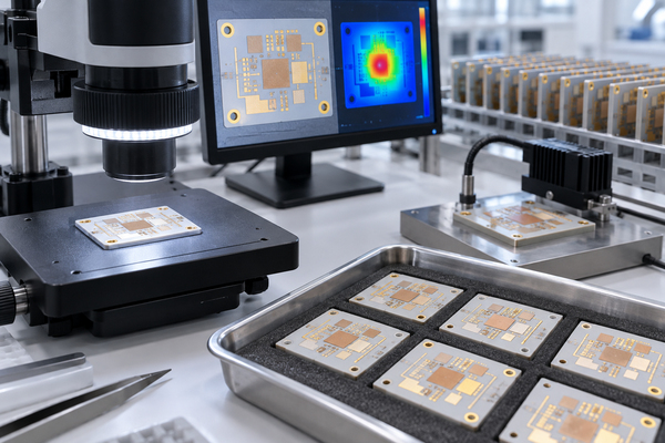
Inspection should be tied to the failure modes of the selected construction. Visual inspection alone cannot verify via continuity, dielectric performance or metal adhesion.
| Requirement | Practical Verification |
|---|---|
| Pattern accuracy | Optical measurement against finished-dimension tolerances |
| Opens and shorts | Electrical continuity and isolation testing |
| Metallized vias | Resistance measurement; cross-section when qualification requires it |
| Copper or metal adhesion | Process-appropriate peel, pull or shear method |
| Flatness or warpage | Defined fixture and measurement condition |
| Assembly surface | Finish thickness, roughness, cleanliness and representative joining trials |
| Thermal-cycle reliability | Test profile based on the module’s materials and operating range |
Sampling level and acceptance criteria should be agreed before quotation. A test name without specimen geometry, temperature range or pass criterion can produce results that are not comparable.
Where Are AlN Ceramic PCBs Used?
AlN circuits are used where electrical isolation and rapid heat removal must fit in a compact structure:
- Power semiconductor modules: IGBT, MOSFET and diode layouts using thick copper for current and heat spreading. Our AlN-capable DBC ceramic substrate for IGBT modules is a relevant manufacturing route for this class of assembly.
- High-power LEDs and laser diodes: submounts and circuits that move heat away from a small die area while providing isolation.
- RF and microwave modules: stable ceramic geometry, controlled conductor patterns and short ground paths.
- Photonic and optoelectronic packages: fine metallization, die attach and wire-bonding surfaces.
- Automotive and industrial power electronics: compact converters, motor drives and high-temperature control assemblies.
Application names do not define the construction. Two IGBT modules can require different ceramics, copper thicknesses and cycling criteria because their die size, baseplate, cooling and operating profile differ.
What Drives AlN Ceramic PCB Cost and Lead Time?
The material premium is only one cost driver. Yield and processing complexity often change the quotation more than board area alone.
Cost and lead time increase with tighter flatness, unusual substrate thickness, thick copper with narrow gaps, small metallized holes, complex outlines, large panels, special finishes, extensive testing and low-volume custom tooling. Over-specification also adds cost: requiring the highest thermal-conductivity grade, the tightest tolerance and full qualification testing without an application need can make a prototype unnecessarily expensive.
Separate must-have requirements from targets. A supplier can then propose a manufacturable tolerance or test plan without weakening the functional requirements.
How Should an AlN Ceramic PCB Manufacturer Be Evaluated?
Evaluate whether the manufacturer can explain the boundary between material capability, circuit fabrication and assembly. A useful response should identify the proposed metallization route, key DFM risks, inspection method and any assumptions behind the quotation.
Ask for evidence relevant to the requested construction, such as representative cross-sections, conductor-thickness control, dimensional measurement or bond testing. A supplier that manufactures DPC does not automatically have the same process window for DBC, AMB or thin film. The review should also distinguish a standard production capability from a special process that needs engineering validation.
What Information Is Needed for a Manufacturing Quote?
Provide enough information to quote the finished construction rather than only the ceramic name:
- Gerber or ODB++ data and a dimensioned mechanical drawing;
- AlN grade or required thermal conductivity, substrate thickness and size;
- process preference, if fixed: DPC, DBC, AMB, thick film or thin film;
- finished copper or metal-stack thickness and surface finish;
- line, gap, hole, via and copper-to-edge requirements;
- flatness, warpage, roughness and cosmetic limits that affect function;
- solder, die-attach or wire-bonding process and peak temperatures;
- operating voltage, temperature range, power or heat-load information;
- test methods, acceptance criteria, quantity and prototype schedule.
Mark critical-to-quality dimensions instead of assigning the tightest tolerance to every feature. If the process is not fixed, describe the electrical, thermal and assembly targets so the manufacturing team can compare suitable routes.
FAQ
Is AIN the Correct Chemical Formula for Aluminum Nitride?
No. The correct formula is AlN, using a lowercase “l” for aluminum and an uppercase “N” for nitrogen. “AIN ceramic PCB” is a common search and typing variation, so both forms may appear in purchasing communication, but technical drawings should use AlN.
What Thermal Conductivity Should Be Specified for an AlN PCB?
Specify the grade required by the thermal model and the verification condition. Commercial electronic substrate grades often fall around 150–180 W/mK, while some grades are higher. Do not substitute a catalog maximum for the guaranteed production value.
Is DBC Better Than DPC for AlN Ceramic PCBs?
Neither is universally better. DBC is suited to thick copper and high current; DPC supports plated, patterned copper and appropriate via structures. Feature size, copper thickness, current, thermal cycling and assembly determine the better fit.
Can AlN Ceramic PCBs Be Wire Bonded?
Yes, when the pad stack, finish, roughness and cleanliness are designed for the selected wire and bonding process. Confirm bondability with representative pull or shear testing after the intended thermal exposure.
Moving from Design to Production
Reliable AIN ceramic PCB manufacturing services connect AlN material selection to metallization, geometry, assembly and verification. A useful quotation package identifies functional requirements and critical tolerances while leaving room for process-specific DFM feedback.
For an AlN ceramic PCB prototype or production review, send your drawings, stack requirements, assembly method and test criteria to sales@bstceramicpcb.com.
 Products
 About us
 Contact us



