






















































 HOME


-

Ceramic PCB for Humanoid Robot joint actuators
2026 04,07 -
LTCC PCB Surprises: What Most People Miss
2025 12,09 -
Step-by-Step Guide to DPC PCB Design for Sensor Systems
2025 12,03 -
Ceramic PCBs Essential Benefits and Applications
2025 12,01 -
How Al2O3 DPC Ceramic Substrate PCB Enhances Heat Dissipation in Modern Electronics?
2025 11,28 -
How to Choose Between Ceramic, FR4, and Metal Core PCBs
2025 11,27 -
DPC Ceramic PCB Materials: Surprising Science Inside
2025 11,26 -
Wire bondable 2-layer Alumina substrates PCB | Bstceramic PCB
2025 09,22 -
Silicon Nitride Substrate, Silicon Nitride Ceramic Substrate Formula
2025 05,08 -
What is thick film ceramic PCB?
2023 08,02
What Should You Specify for an AlN Submount for Surgical Laser Systems?
Published:
An AlN submount for surgical laser systems sits between a laser diode die and the package heat-spreading structure. It must provide electrical insulation, a controlled thermal path and a metallized surface compatible with die attach and wire bonding. It is not a complete surgical laser module, and selecting AlN alone does not establish optical output, lifetime or medical-device compliance.

What Is an AlN Submount for Surgical Laser Systems?
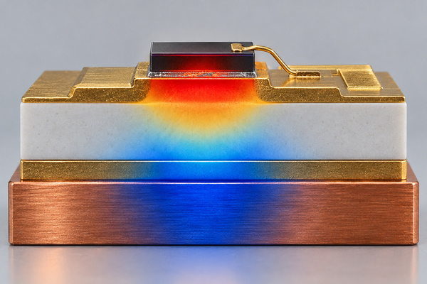
An AlN submount is a small aluminum nitride ceramic carrier with patterned metallization. In a chip-on-submount laser diode assembly, the die is attached to a metallized pad, electrical connections are completed by the rear contact and/or wire bonds, and heat flows through the die attach, metallization, ceramic and package base.
The word surgical describes the end system, not a special ceramic composition. A laser diode submount used in a surgical source still needs an application-specific drawing covering wavelength-independent mechanical features, pulse or continuous-wave operation, cooling arrangement, package atmosphere, sterilization boundary and acceptance tests. A TO can laser diode, a bar, a single emitter and a fiber-coupled module can require different pad and heat-flow geometries even when they all use AlN material.
Why Is AlN Used Under a Laser Diode?
Aluminum nitride combines electrical insulation with much higher bulk thermal conductivity than common alumina grades. Its coefficient of thermal expansion is also relatively close to semiconductor materials. These properties can reduce the thermal and mechanical mismatch between a laser die and a metal heat spreader.
Those benefits apply only when the complete interface is controlled. A voided solder layer, insufficient metallized area or poor contact to the next heat spreader can dominate the temperature rise. For an AlN laser diode submount, we therefore review the ceramic, conductor geometry, die-attach system and downstream mounting interface as one assembly rather than treating the ceramic datasheet as the finished thermal result.
Why Does Thermal Resistance Matter More Than One Conductivity Number?
Bulk conductivity is a material input; thermal resistance is a property of the built heat path. For a simplified one-dimensional layer, resistance increases with thickness and decreases with the effective heat-transfer area. The real package also contains spreading resistance and interface resistance, so a single W/mK value cannot predict junction temperature.
| Part of the heat path | Information needed | Typical design risk |
|---|---|---|
| Laser die | Heat-source size and power profile | Local heat flux is hidden by average power |
| Die attach | Material, thickness, coverage and void limit | Voids or excessive bond-line thickness increase resistance |
| Top metallization | Pad area, metal stack and solderability | A small or poorly wetted pad constricts heat flow |
| AlN ceramic | Grade, thickness and dimensional data | Generic AlN property values are substituted for the selected grade |
| Bottom metallization/interface | Area, finish and mounting process | The lower interface is omitted from the model |
| Package base/cooler | Material, flatness, clamp or solder condition | Package assumptions do not match the prototype |
For pulsed laser operation, peak and transient temperature may matter even when average power appears acceptable. The customer should provide the operating waveform and cooling boundary so the thermal model and prototype measurement use the same conditions.
Which AlN Grade and Thickness Should Be Specified?
Commercial AlN grades do not share one universal conductivity, dielectric value, grain structure or surface condition. The purchase drawing should identify the approved material grade or the minimum properties that must be documented. If a grade substitution is allowed, define which properties require revalidation.
Thickness is a trade-off. A thinner ceramic shortens the through-thickness path and can reduce package height, but it can be harder to handle and may offer less mechanical margin during assembly. A thicker part can improve handling while increasing thermal path length. The correct value depends on die size, package support, metallization stress, flatness and the method used to separate the submounts.
Our double-sided AlN DPC ceramic circuit is a relevant product reference for projects that need aluminum nitride with patterned conductors on both faces. The linked configuration is not a default surgical-laser design; we use the customer's drawing and assembly inputs to determine whether that material and process route fit the submount.
How Should the Die-Attach Material Be Selected?
Die attach must be selected together with the die backside metallization, submount finish, reflow profile and reliability target. Eutectic AuSn can provide a thin, stable metallic joint when the mating surfaces and process are designed for it. Indium or another compliant metallic attach can help accommodate stress in a suitable package. Conductive epoxy may lower processing temperature but introduces a different thermal path, cure process and aging behavior.
No attach material is universally best. The drawing should state whether pre-deposited solder is required, its alloy and pattern, the allowed bond-line or void criteria, and whether die shear or cross-section testing belongs in qualification. If the die-attach process is performed by the customer, the submount finish still has to be compatible with that process.
How Should the Metallization Stack Be Selected?
The metallization stack has several jobs: adhere to AlN, carry current, support solder or eutectic bonding, provide a wire-bondable surface where needed, and remain stable through assembly temperatures. The words gold plated are not a complete specification. The base metallization, barrier layer, top finish, thickness range, pattern geometry and inspection method must be defined.
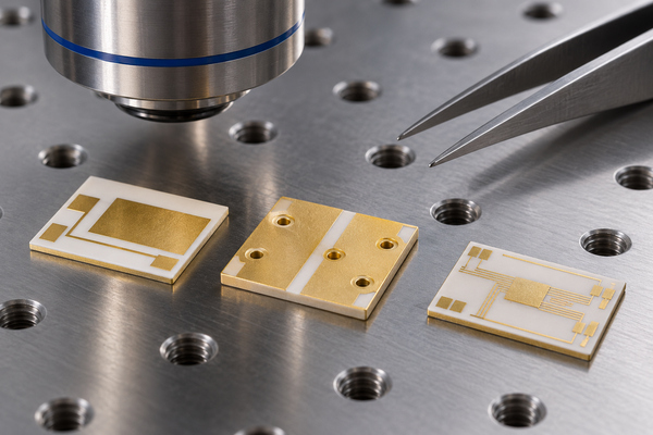
DPC can support patterned copper, plated vias and double-sided routing for compact ceramic circuits. Thin-film processing is relevant when the design needs finer, controlled metallization and precision pads. Our laser-equipment DPC ceramic circuit shows the laser-equipment context of a patterned ceramic circuit, while the final material, copper structure and finish for a surgical source remain drawing-specific.
If AuSn is deposited on the submount, define alloy, area, thickness and storage/handling requirements. If gold is intended for wire bonding, define wire material and bonding method rather than assuming that every gold finish is equivalent.
How Do Flatness, Surface Roughness and Edge Quality Affect Assembly?
Flatness influences bond-line consistency and contact with the next heat-spreading surface. Surface roughness affects metallization, die-attach wetting and the ability to form a controlled thin interface. Edge chips can remove mechanical support or approach active conductors on a small submount.
These requirements need a measurement definition, not only a limit. State the datum, measured area, sampling plan and whether the value applies to bare ceramic, metallized submount or a selected pad region. Surface finish can differ between as-fired, lapped and polished AlN, so the drawing should connect the surface condition to the assembly operation it supports.
Which Pad, Ground and Wire-Bond Features Belong in the Layout?
The layout must show the die footprint, polarity, current path, ground or return structure, wire-bond pads, probe access and keep-outs. Short, wide current paths can reduce electrical and thermal constriction, but optical access, bond-tool clearance and isolation still need space. For a chip-on-submount laser diode, the die edge and emitting facet also need a clear mechanical relationship to the submount edge.
Wire-bond pads should be sized and positioned for the selected wire and bonding process. The design should state whether a pad is for die attach, wire bonding, soldering, probing or package attachment. Combining these functions without a defined process can create finish and geometry conflicts.
Our thin-film ceramic circuit for medical equipment is relevant when a medical assembly needs precision metallization and compact interconnection. It supports the manufacturing route discussed here; it is not evidence that the finished laser system has completed medical certification.
How Should CTE and Mechanical Stress Be Managed?
AlN can reduce expansion mismatch with semiconductor dies, but the package is a multi-material stack. Copper, gold, solder, die material, ceramic and the package base expand differently. Large copper imbalance, thick plated areas, rigid joints or an unsupported thin ceramic can distort the assembly during heating and cooling.
Use symmetric structures where the electrical design allows, avoid abrupt metal-area transitions near the die, and evaluate the attach layer and package base together. A room-temperature flatness result does not replace thermal-cycle validation. If the submount is clamped rather than soldered, contact pressure and support geometry also become part of the mechanical design.
What Changes for Pulsed and Continuous-Wave Surgical Lasers?
A continuous-wave source creates a sustained heat load, so steady-state thermal resistance and cooler capacity are central. A pulsed source can create high local peak temperature and repeated thermo-mechanical strain even when its average power is lower. Pulse width, repetition rate, duty cycle and peak electrical input should therefore be recorded separately.
The operating mode can also change the acceptance plan. A short prototype test may reach steady state for one design but miss cumulative cycling stress in another. Submount inspection should be paired with module-level temperature, optical stability and life testing under the actual drive profile.
Which Manufacturing Route Fits the Submount?
The route depends on feature size, conductor thickness, via requirements, solder deposition and volume. DPC is useful for patterned copper and plated interconnects. Thin film supports fine metallization and precision resistor or conductor features when the stack is designed for that process. Other metallization systems may be suitable for simpler pads or different attachment methods.
We begin with the assembly function, then review AlN grade, outline, thickness, pad geometry, via structure, finish and singulation. We do not select a process from the application name alone. The term surgical laser submount can mean a simple two-pad carrier, a double-sided ceramic circuit or a more integrated routing structure.
What Should Prototype Inspection and Validation Cover?
Incoming and in-process checks should match the drawing and the assembly risk. A practical plan can include:
- finished outline, thickness, flatness and edge-chip limits;
- conductor registration, line/space, pad dimensions and via continuity;
- metallization and finish thickness where specified;
- surface condition, contamination and solder-deposit geometry;
- electrical continuity and isolation for patterned circuits;
- die-attach coverage, voiding and shear strength during assembly qualification;
- thermal and optical performance in the representative package.
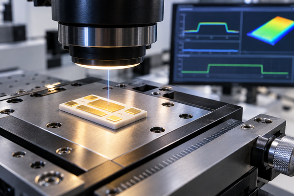
A microscope image alone cannot verify flatness or metallization thickness. Conversely, a material certificate cannot show pad registration or edge damage. Each acceptance item needs a method, sampling rule and pass/fail limit.
What Must Be Validated at the Medical-System Level?
The ceramic submount is one component in a surgical laser system. The device manufacturer or system integrator must validate optical power and beam delivery, electrical safety, thermal protection, software and controls, biocompatibility where applicable, sterilization boundaries, risk management and the regulatory requirements for the intended market.
Our manufacturing review can support a controlled ceramic drawing, material documentation and submount inspection plan. It cannot by itself establish that the assembled laser source is safe or approved for a surgical procedure. Keeping this boundary explicit prevents a component specification from being mistaken for system certification.
What Information Should Be Included in the RFQ?
To review and quote a custom submount without guessing, send us:
- dimensioned drawing plus Gerber, ODB++, DXF or another suitable circuit file;
- AlN grade or required material properties, thickness and tolerances;
- die size, heat-source area and intended package architecture;
- metallization stack, conductor thickness and wire-bond requirements;
- die-attach material, solder-deposit requirements and assembly temperature;
- flatness, roughness, edge-chip and surface-cleanliness criteria;
- pulse or continuous-wave operating profile and cooling boundary;
- inspection, traceability and qualification requirements;
- prototype and production quantities.
At BSTCeramicPCB, we use these inputs to review the ceramic, metallization, panel method and inspection plan before quotation. Email the drawing and specification to sales@bstceramicpcb.com. Items that are still under development should be marked as open decisions so they can be resolved during engineering review rather than hidden behind a generic tolerance.
An AlN submount for surgical laser systems should be purchased as a defined thermal and interconnection component, not as an unspecified ceramic plate. The most useful drawing connects material grade, thickness, metal stack, die attach, surface condition and acceptance tests to the actual laser package and operating profile.
 Products
 About us
 Contact us



