






















































 HOME
HOME

-

Ceramic PCB for Humanoid Robot joint actuators
2026 04,07 -
LTCC PCB Surprises: What Most People Miss
2025 12,09 -
Step-by-Step Guide to DPC PCB Design for Sensor Systems
2025 12,03 -
Ceramic PCBs Essential Benefits and Applications
2025 12,01 -
How Al2O3 DPC Ceramic Substrate PCB Enhances Heat Dissipation in Modern Electronics?
2025 11,28 -
How to Choose Between Ceramic, FR4, and Metal Core PCBs
2025 11,27 -
DPC Ceramic PCB Materials: Surprising Science Inside
2025 11,26 -
Wire bondable 2-layer Alumina substrates PCB | Bstceramic PCB
2025 09,22 -
Silicon Nitride Substrate, Silicon Nitride Ceramic Substrate Formula
2025 05,08 -
What is thick film ceramic PCB?
2023 08,02
Alumina Ceramic Substrate Fabrication from Powder to Circuit
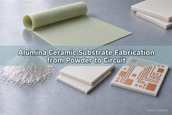
Alumina ceramic substrate fabrication turns aluminum oxide powder into a dense insulating plate, then adds the geometry, surface condition and metallization needed by an electronic circuit. The critical link is between these stages: firing determines the ceramic body, finishing establishes usable dimensions, and metallization creates the electrical connections. At BSTCeramicPCB, our ceramic circuit work connects substrate selection with DPC, thick-film and thin-film processing for the intended assembly.
What Does Alumina Ceramic Substrate Fabrication Include?
Fabrication includes two distinct routes: producing the ceramic blank and producing a circuit on that blank. An alumina ceramic substrate is a rigid, electrically insulating aluminum oxide body; it does not become a PCB simply by being cut to size.
For a conventional single- or double-sided circuit, the ceramic is usually fired before metal patterns are added. Co-fired ceramic packages follow a different sequence: conductive features and vias can be formed in green ceramic layers before lamination and firing. These routes have different conductor choices, shrinkage controls and design rules. A post-fired DPC process should not be treated as a substitute for a multilayer co-fired package process.
Which Alumina Grade Fits the Circuit Process?
Choose the grade together with the intended metallization and surface specification. Purity alone does not establish flatness, roughness, thermal performance or the minimum printable feature size.
| Material choice | Practical circuit use | What still needs definition |
|---|---|---|
| 96% alumina | A common base for thick-film circuits and DPC boards | Finished thickness, surface condition, conductor system and assembly requirements |
| Higher-purity alumina, such as 99.6% | Often selected for thin-film and precision electronic substrates | Surface finish, porosity, dielectric data at the operating frequency and dimensional requirements |
| Co-fired alumina formulation | Multilayer packages with buried conductors or filled vias | Tape system, compatible conductive paste and shrinkage compensation |
Alumina substrate properties should be taken from the selected grade, not a mixed-material ceramic brochure. For example, a thermal-conductivity range that includes AlN cannot be applied to an Al2O3 plate. Likewise, bulk dielectric strength is not the operating-voltage rating of a completed circuit with exposed conductor gaps.
How Are Powder Preparation and Forming Controlled?
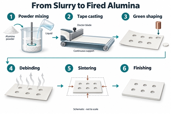
Powder preparation controls how uniformly the ceramic packs before firing. Particle size distribution, additive content and dispersion affect green density; binder and solvent systems control forming and handling. Trapped air or agglomerates can become local defects that later polishing cannot reliably eliminate.
Tape casting is suited to thin, broad sheets. A slurry passes beneath a doctor blade, dries on a carrier and becomes a handleable green tape. The blade gap is a process setting, not the final fired thickness. Dry pressing is another route for plate-like parts; the preferred method depends on geometry, thickness and production requirements.
Green-state punching or shaping creates holes and outlines while the material is easier to work. For electronic alumina substrates, the layout must reserve enough material around openings to survive handling and firing. This is why a hole pattern and an outline should be developed as one geometry rather than as unrelated operations.
What Happens During Debinding and Sintering?
Debinding removes the organic ingredients used to form the green part; sintering bonds the ceramic particles and reduces porosity. Removing organics too quickly can leave internal pressure, cracks or residual contamination. During densification, the body shrinks, and uneven density or support conditions can produce distortion.
The firing cycle must match the powder formulation, part thickness and furnace loading. There is no single temperature or shrinkage percentage that should be copied into every alumina drawing. Compensating green dimensions requires the qualified material and process, including separate consideration of in-plane and thickness changes.
For a post-fired circuit, the important handoff is a ceramic blank that meets the agreed dimensional and surface condition before metallization. Subsequent paste firing, metal bonding or thermal processing adds another exposure, so flatness should also be considered at the finished-circuit stage.
Should Holes and Outlines Be Machined Before or After Firing?
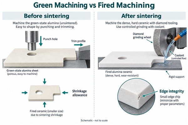
Create features before firing when efficient shaping matters and the final tolerance can accommodate controlled shrinkage. Use fired-state machining when a critical final dimension must be established after shrinkage has occurred.
| Operation | Best reason to use it | Main limitation |
|---|---|---|
| Green punching or machining | Form holes, windows and profiles before the ceramic becomes hard | Dimensions change during firing; fragile green features need support |
| Diamond grinding or dicing | Establish accurate dimensions on dense alumina | Edge damage, tooling wear and machining time must be controlled |
| Laser drilling, cutting or scribing | Produce selected holes, profiles or separation lines | Taper, recast material and heat-affected damage depend on the laser process |
Fired alumina is hard but brittle. Ordinary FR4 routing assumptions do not transfer directly, and a material described as a machinable glass ceramic is not equivalent to dense alumina. Minimum hole size and edge distance must be tied to ceramic thickness and the actual machining method.
How Do Thickness, Flatness and Roughness Differ?
Thickness defines the distance between opposing surfaces. Flatness describes how far a surface departs from a plane. Roughness describes much smaller surface texture. Specifying one does not control the other two.
A bowed plate can have consistent local thickness yet leave an uneven bond line against a heat spreader. A flat plate can still be too rough for a fine deposited conductor. Lapping, grinding and polishing serve different finishing objectives, and they also change the remaining ceramic thickness.
For our thin-film ceramic circuits for wireless communication, the published substrate-roughness capability is Ra at or below 0.1 micrometer, with 0.05 micrometer listed for special needs. These are process-specific capabilities to review against the design, not a requirement for every alumina board. The same polishing requirement can be unnecessary for a less demanding printed circuit.
How Is the Electrical Circuit Added to Alumina?
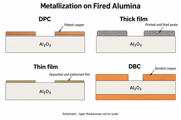
Metallization must match conductor geometry, current, passive elements and the final connection method. The ceramic body provides insulation; the metal system supplies the electrical path.
| Route | How the conductor is formed | Useful fit | Design consequence |
|---|---|---|---|
| DPC, direct plated copper | Deposit an adhesion/seed system, pattern and plate copper, then remove unwanted seed | Defined copper traces and pads on single- or double-sided substrates | Copper thickness, spacing and via coverage are linked |
| Thick film | Screen-print compatible pastes and fire them on the ceramic | Conductors and printed resistors in hybrid circuits | Paste, firing profile and substrate surface must work together |
| Thin film | Deposit metal or resistive films and define features by patterning | Fine geometries and precision RF or analog circuits | Surface quality, film adhesion and dimensional control become especially important |
| DBC, direct bonded copper | Bond copper sheet to ceramic through a controlled high-temperature process, then pattern it | Substrates requiring substantial copper for power circuitry | Thick copper affects etching geometry and thermomechanical stress |
Our 96% alumina DPC substrate for LED chips is a concrete example: a 1.0 mm ceramic board, specified at +/-0.1 mm, with 18 micrometer copper. That is one product construction, not a universal DPC stackup. Surface finishes such as ENEPIG are applied to a compatible metal structure; they do not replace the underlying conductor or ceramic-to-metal adhesion system.
Which Design Details Must Be Fixed Before Circuit Fabrication?
Define the ceramic geometry and metal pattern in a common reference system. Otherwise, individually acceptable features can still misalign when combined.
- Holes and vias: distinguish mechanical openings from plated or filled electrical connections. Include the finished aperture, positional tolerance and required conductor continuity.
- Circuit-to-edge clearance: account for the cutting method, conductor setback and permissible edge damage. An edge chip must not reach a functional conductor or sealing area.
- Thickness definition: state whether the dimension describes the bare ceramic or the total finished metal-and-ceramic stack.
- Assembly interfaces: define die-attach areas, wire-bond pads, solder lands and heat-spreader contact surfaces according to their actual use.
- Copper distribution and mounting: evaluate asymmetric metal coverage and rigid clamping where thermal expansion can load a brittle substrate.
For an alumina substrate PCB, a hole diameter that looks feasible in isolation may leave too little ceramic beside a window or too little annular metal around a via. Review the smallest remaining web and the complete tolerance stack, not only the nominal dimensions.
How Is Fabrication Quality Verified?
Verification should target the failure mechanisms created by the selected route. A material certificate supports grade identification but does not establish finished circuit continuity, adhesion or assembly reliability.
| Risk | Relevant verification | Meaning for the circuit |
|---|---|---|
| Warpage or thickness variation | Dimensional measurement in a defined free or supported condition | Checks assembly fit and contact with the thermal interface |
| Edge chipping or cracks | Optical examination of cut edges, holes and critical regions | Identifies damage near conductors, mounting points or bond areas |
| Poor metal adhesion | An agreed adhesion or bond-strength method for the actual metal stack | Checks the ceramic-to-metal interface rather than appearance alone |
| Open circuits, shorts or via defects | Netlist-based electrical testing and appropriate via inspection | Confirms intended connections and isolation |
| Thermal mismatch | Application-relevant thermal cycling followed by electrical and structural checks | Evaluates the combined ceramic, metal and attachment system |
A prototype should retain production-representative substrate grade, metallization and critical geometry. If the prototype uses a different thickness or conductor system, successful assembly does not validate the final construction. Inspection conditions and acceptance limits should be agreed before testing, especially where optical appearance alone cannot reveal internal damage.
How Does the Fabrication Route Change with the Application?
The useful route is the one that supports the circuit's dominant requirement without adding unnecessary processing.
An LED substrate needs an electrically isolated thermal path and pads compatible with the selected chip connection. A thin-film RF circuit places greater emphasis on surface quality, conductor geometry and dielectric behavior at its operating frequency. A thick-film sensor or hybrid circuit may need printed resistors and conductors processed as a compatible paste system.
Our alumina thick-film circuits for medical electronics include a two-layer, 96% Al2O3 construction with 10-15 micrometer AgPd conductors. This illustrates a different manufacturing route from the copper LED board; neither construction should be selected solely because both use alumina. Device qualification remains a separate requirement from fabricating its ceramic circuit.
The practical goal of alumina ceramic substrate fabrication is a finished substrate whose geometry, surface and metal system support the intended assembly. To discuss a ceramic circuit with BSTCeramicPCB, send your drawing, proposed stackup and application requirements to sales@bstceramicpcb.com. We can review the relevant circuit route without treating every design as the same alumina plate.
 Products
 About us
 Contact us



