






















































 HOME


-

Ceramic PCB for Humanoid Robot joint actuators
2026 04,07 -
LTCC PCB Surprises: What Most People Miss
2025 12,09 -
Step-by-Step Guide to DPC PCB Design for Sensor Systems
2025 12,03 -
Ceramic PCBs Essential Benefits and Applications
2025 12,01 -
How Al2O3 DPC Ceramic Substrate PCB Enhances Heat Dissipation in Modern Electronics?
2025 11,28 -
How to Choose Between Ceramic, FR4, and Metal Core PCBs
2025 11,27 -
DPC Ceramic PCB Materials: Surprising Science Inside
2025 11,26 -
Wire bondable 2-layer Alumina substrates PCB | Bstceramic PCB
2025 09,22 -
Silicon Nitride Substrate, Silicon Nitride Ceramic Substrate Formula
2025 05,08 -
What is thick film ceramic PCB?
2023 08,02
Alumina CTE Explained: Thermal Expansion in Ceramic PCBs
Published:
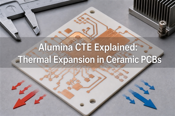
Alumina CTE describes how much an alumina ceramic changes length as its temperature changes. For ceramic PCB engineers, the number is useful only when it is tied to a material grade, a temperature interval, and the copper, semiconductor, solder, or baseplate that constrains the substrate.
What Is Alumina CTE?
CTE means coefficient of thermal expansion. For an alumina substrate, it is normally reported as a linear value in ppm/K, ppm/°C, or ×10⁻⁶/K. A value of 7 ppm/K means that a free, unconstrained alumina part changes length by about 7 micrometers per meter for each 1 K temperature change.
The numerical increment is the same in ppm/K and ppm/°C because a change of 1 K equals a change of 1°C. CTE is not thermal conductivity. Thermal conductivity describes how quickly heat moves through the ceramic; CTE describes the dimensional response after temperature changes.
What Is the Typical CTE of Alumina?
Electronic-grade alumina substrates commonly fall near 6.8 to 7.2 ppm/K in manufacturer data measured across defined temperature ranges. A broader value may be appropriate for other formulations or wider temperatures, but it should not replace the grade-specific data sheet used for a real design.
| Alumina grade example | Representative CTE | Reported interval | Engineering note |
|---|---|---|---|
| 96% alumina | 7.0 × 10⁻⁶/K | 40-400°C | Common substrate grade; confirm the actual formulation |
| 97% alumina | 7.0 × 10⁻⁶/K | 40-400°C | Similar nominal value does not imply identical strength or surface properties |
| 99% alumina | 6.8 × 10⁻⁶/K | 40-400°C | Higher purity does not automatically mean a higher CTE |
| 99.6% alumina | 7.2 × 10⁻⁶/K | 40-400°C | Grade chemistry and microstructure still matter |
These are representative supplier values, not universal limits. The practical rule is to specify the exact substrate grade and use its declared interval instead of assuming that alumina purity alone determines expansion.
How Do You Calculate Thermal Expansion?
For a first-order estimate, use:
ΔL = α × L₀ × ΔT
where ΔL is the change in length, α is the linear CTE, L₀ is the starting length, and ΔT is the temperature change.
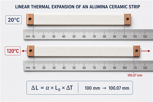
For example, a 100 mm alumina substrate with a CTE of 7 ppm/K heated through 100 K expands by approximately 0.07 mm if it is free to move. That small change becomes important when copper, silicon, solder, or a metal baseplate tries to expand by a different amount.
For two bonded materials, a useful screening estimate is Δε ≈ (α₁ − α₂) × ΔT. This mismatch strain is not the final stress. Elastic modulus, layer thickness, pad geometry, bondline compliance, edge distance, assembly constraint, dwell time, and cycle count determine where stress accumulates.
Why Does the Temperature Range Matter?
CTE is temperature-dependent. A data sheet may report an average CTE from 20-300°C or 40-400°C, while another source may give an instantaneous value at one temperature. Those numbers are not directly interchangeable.
For ceramic PCB work, use the interval that covers assembly and service conditions. A module that sees solder reflow and then operates from -40°C to 150°C should not be evaluated only with a room-temperature value. The design review should separate three events:
- assembly heating, where copper, ceramic, solder, and components are joined;
- operating excursions, where the module repeatedly heats and cools;
- qualification cycles, which may exceed normal operation to reveal fatigue or edge defects.
If the supplier data covers a different interval, request the curve or the average CTE for the relevant range. Do not extrapolate a single number far beyond its stated conditions.
How Do 96%, 99%, and 99.6% Alumina Compare?
Purity affects more than CTE. It can change thermal conductivity, dielectric behavior, surface finish, mechanical properties, firing behavior, and cost. However, the representative values above show why purity should not be used as a shortcut for expansion: 99% alumina may have a slightly lower declared CTE than both 96% and 99.6% grades.
Choose a grade by the complete requirement set. A 96% alumina substrate can be appropriate when the metallization process, mechanical loading, insulation, thermal path, and cost targets are satisfied. A high-purity grade is justified when its verified property package solves a defined requirement, not simply because its purity number is larger.
How Does Alumina CTE Compare with Copper, Silicon, AlN, Si3N4, and FR4?
The useful comparison is the CTE difference between bonded materials, not which isolated material has the smallest number.
| Material | Representative CTE behavior | Practical implication in electronics |
|---|---|---|
| Alumina | about 6.8-7.2 ppm/K for common electronic grades | Moderate match to some package metals; lower expansion than copper |
| Copper | about 16.5-17 ppm/K | Drives shear and edge stress when bonded to alumina |
| Silicon | about 2.6 ppm/K near room temperature; average rises with temperature | Die attach and large die geometry need attention |
| Aluminum nitride (AlN) | about 4.5-4.7 ppm/K | Closer to silicon and much higher thermal conductivity than alumina |
| Silicon nitride (Si3N4) | roughly 2.8-3.4 ppm/K, grade-dependent | Low expansion and high mechanical toughness can benefit power modules |
| FR4 | in-plane commonly around the mid-teens; z-axis is much higher and grade-dependent | Anisotropic expansion makes direct comparison with isotropic ceramics incomplete |
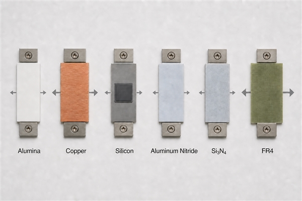
The table is a screening tool. Final material selection still needs the exact grade, temperature interval, layer orientation, and assembly geometry.
How Does CTE Mismatch Affect Ceramic PCBs?
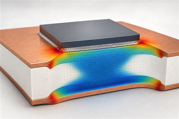
When bonded layers expand differently, the assembly bends or develops interfacial stress. In ceramic PCBs, the highest-risk locations are often copper corners, ceramic edges, large soldered pads, die corners, vias near cutouts, and areas where the copper distribution is strongly asymmetric.
Common failure modes include solder fatigue, copper lift, metallization cracking, ceramic edge cracks, die-attach degradation, and warpage that interferes with assembly. A crack does not prove that the ceramic CTE was “wrong.” It may indicate an abrupt copper corner, excessive metal imbalance, poor edge clearance, a rigid attachment, a voided bondline, or an unsuitable thermal cycle profile.
How Do DBC, DPC, and Thick-Film Constructions Change Thermal Stress?
The same alumina grade can behave differently after metallization because metal thickness and bonding method change the stiffness and constraint of the composite.
| Construction | Metal structure | CTE-related design focus |
|---|---|---|
| DBC | Relatively thick bonded copper, often on both sides | Copper balance, corner radii, edge clearance, ceramic thickness, and baseplate attachment |
| DPC | Plated copper with finer features and generally lower metal mass | Local current density, plated thickness transitions, via regions, and large-pad asymmetry |
| Thick film | Fired conductive paste and optional resistor/dielectric layers | Paste system, firing compatibility, conductor geometry, and attached component footprint |
For a DPC design, a real single-sided alumina DPC ceramic circuit board illustrates why copper distribution matters: a single metal face creates a different bending condition from a balanced two-sided stack. Sensor layouts on a 96% Al2O3 DPC ceramic substrate also need clearance around edges and local features rather than a substrate-only CTE check.
In thick-film assemblies, conductor paste is thinner and mechanically different from bulk copper, but thermal mismatch remains relevant at large pads and component joints. A 96% Al2O3 thick-film ceramic substrate should therefore be reviewed as a fired multilayer system, not as bare alumina alone.
What Design Choices Reduce CTE-Related Failures?
Start with geometry and constraint before changing the ceramic grade. The following actions usually provide more direct control over stress:
- balance copper area and thickness on opposing faces when the electrical design permits;
- replace sharp copper corners with suitable radii and avoid abrupt thickness transitions;
- keep high-stress metal features away from ceramic edges, slots, and laser-cut corners;
- segment very large copper areas when current and thermal spreading requirements allow;
- select a substrate thickness that supports the assembly without creating unnecessary stiffness;
- control solder or sinter bondline thickness and voiding under large components;
- include the baseplate, fasteners, thermal interface material, and enclosure constraint in the mechanical model;
- validate the actual stack with thermal cycling, warpage measurement, cross-sectioning, and electrical checks.
Simulation is most useful when it includes temperature-dependent material data and realistic boundary conditions. A colorful stress plot built from generic room-temperature constants can be less informative than a simpler model using verified layer thicknesses and assembly constraints.
How Should Alumina CTE Be Specified and Verified?
A useful drawing or material specification identifies the alumina grade or approved material family, nominal purity, substrate thickness, CTE value with temperature interval, test method or supplier data-sheet reference, and the permitted substitution process. Writing only “alumina, CTE 7 ppm/K” leaves too much ambiguity.
For a new ceramic PCB, the engineering package should also identify copper or metallization thickness, pattern files, finish, component and die-attach materials, operating temperature range, assembly peak temperature, baseplate material, mounting constraint, and required thermal-cycle profile. These inputs allow the substrate, metallization, and assembly to be reviewed as one system.
During qualification, compare certificates and lot data with the approved grade, but do not rely on a certificate alone to predict assembly life. Dimensional inspection, flatness, adhesion, thermal cycling, cross-sections, and functional testing reveal manufacturing and geometry effects that a bulk CTE value cannot capture.
FAQ
What is CTE of alumina?
Common electronic alumina grades are often around 6.8-7.2 ppm/K over a declared temperature interval. Always use the value for the exact grade and range in the supplier data.
Is alumina the same as aluminum?
No. Alumina is aluminum oxide ceramic, Al2O3. Aluminum is a metal with a much higher CTE, roughly in the low-20s ppm/K depending on alloy and temperature.
Is ppm/K the same as ppm/°C for CTE?
Yes for temperature differences. A 1 K change and a 1°C change have the same magnitude, so the numerical CTE value is unchanged.
Does higher alumina purity always reduce CTE?
No. Representative grade data does not show a simple monotonic relationship. Additives, porosity, microstructure, and the measurement interval also affect the reported value.
Why is copper-alumina CTE mismatch important?
Copper expands more than alumina. When bonded, the difference creates strain that can drive warpage, copper-edge stress, solder fatigue, or ceramic cracking during temperature changes.
Is alumina CTE lower than AlN?
No. Typical AlN CTE is around 4.5-4.7 ppm/K, below common alumina values near 7 ppm/K. AlN is also much more thermally conductive, but it normally costs more and has different processing considerations.
Can one room-temperature CTE value predict thermal-cycle life?
No. It is only an input. Cycle range, dwell time, ramp rate, layer thickness, elastic properties, geometry, bondline quality, and mechanical constraints also control life.
What data should be used in a thermal simulation?
Use grade-specific, temperature-dependent CTE and modulus data where available. Include copper, ceramic, die, solder or sinter layer, baseplate, thermal interface, and realistic mounting constraints.
Conclusion
Alumina CTE is usually close to 7 ppm/K for electronic substrate grades, but the design decision cannot stop at that number. Confirm the grade and temperature interval, compare every bonded material, and evaluate the complete metallized stack under realistic assembly and service cycles.
BSTCeramicPCB can review alumina substrate grade, metallization structure, copper balance, layer thickness, and thermal-cycle requirements before prototype release. For an engineering review, contact sales@bstceramicpcb.com.
 Products
 About us
 Contact us



