






















































 HOME


-

Ceramic PCB for Humanoid Robot joint actuators
2026 04,07 -
LTCC PCB Surprises: What Most People Miss
2025 12,09 -
Step-by-Step Guide to DPC PCB Design for Sensor Systems
2025 12,03 -
Ceramic PCBs Essential Benefits and Applications
2025 12,01 -
How Al2O3 DPC Ceramic Substrate PCB Enhances Heat Dissipation in Modern Electronics?
2025 11,28 -
How to Choose Between Ceramic, FR4, and Metal Core PCBs
2025 11,27 -
DPC Ceramic PCB Materials: Surprising Science Inside
2025 11,26 -
Wire bondable 2-layer Alumina substrates PCB | Bstceramic PCB
2025 09,22 -
Silicon Nitride Substrate, Silicon Nitride Ceramic Substrate Formula
2025 05,08 -
What is thick film ceramic PCB?
2023 08,02
AMB Substrate for Traction Inverter: What Makes It Assembly-Ready?
Published:
An AMB substrate for traction inverter is assembly-ready when the delivered ceramic circuit matches the module process at every critical interface: active braze, etched copper, die-attach surface, dimensional datum, flatness area and incoming-inspection plan. Selecting Si3N4 and thick copper does not finish the specification. The manufacturer and module assembler need one controlled acceptance package.
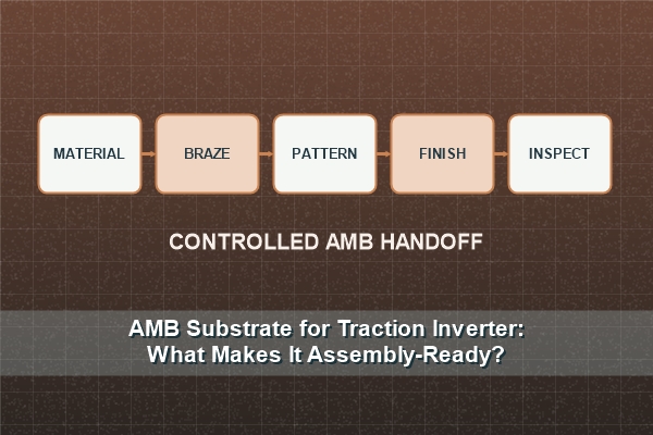
What Does “Assembly-Ready” Mean for an AMB Substrate?
Assembly-ready means the substrate can enter the customer's qualified joining and interconnection flow without an unresolved material, geometry or cleanliness decision. The released drawing should define ceramic grade, finished copper thickness, pattern, surface finish, datums, functional flatness area, edge condition and test requirements.
It does not mean that the bare substrate is already qualified as an inverter module. Die attach, wire or clip bonding, baseplate attach and cooling remain downstream processes, but their needs must be translated into substrate characteristics before manufacture.
How Is the AMB Circuit Manufactured?
The AMB route has a distinct manufacturing sequence:
- Confirm the ceramic, copper and active-braze construction.
- Prepare and clean the joining surfaces.
- Braze copper to the ceramic under the specified atmosphere and thermal cycle.
- Pattern the bonded copper by imaging and etching.
- Apply the required surface finish and final clean.
- Inspect pattern, dimensions, flatness, finish and agreed interface evidence.
- Package the substrates to protect the assembly surfaces and edges.
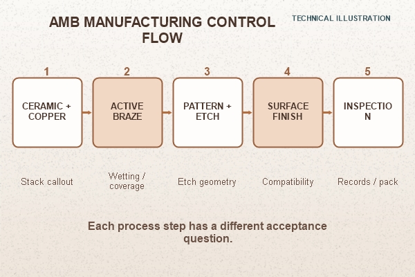
Each stage creates a different control point. A good final outline does not compensate for poor braze coverage, and a sound braze does not compensate for an over-etched die pad.
Which Active-Braze Defects Affect Later Assembly?
The interface should be evaluated by defect mechanism rather than by a generic “bond looks good” statement.
| Potential condition | Assembly or reliability consequence | Useful evidence |
|---|---|---|
| Incomplete wetting or reaction | Reduced bonded area and local stress concentration | Process record plus targeted cross-section |
| Entrapped void or discontinuity | Local thermal and mechanical weakness | Qualified non-destructive method or sectioning plan |
| Excess or uneven braze flow | Geometry interference or variable interface | Edge inspection and controlled coupon |
| Contamination | Inconsistent reaction or finish adhesion | Cleaning control and surface inspection |
| Ceramic edge damage | Crack initiation during handling or attach | Magnified visual inspection with agreed limits |
The inspection method must be matched to the critical area. One coupon cannot prove the entire production panel unless the sampling relationship is defined.
How Should Ceramic and Copper Callouts Be Released?
Specify finished values and acceptable variation, not only starting foil or nominal ceramic stock. Copper thickness affects current capacity, etch shape and mechanical loading. Ceramic thickness affects thermal resistance, stiffness and handling. The active-braze system should be identified to the level required for process control without copying a supplier's confidential formulation into the customer drawing.
Our AMB ceramic substrate for IGBT power modules is the direct product route for this construction. We review the material stack and pattern together because an acceptable laminate can still become an unsuitable finished circuit after aggressive etching or unbalanced copper removal.
What Copper Geometry Survives Etching and Module Assembly?
Large die pads, narrow gate features, power terminals and copper-to-edge clearances have different manufacturing risks. Etching thick copper produces sidewall geometry that must be allowed for in the artwork. Sharp re-entrant corners and abrupt changes in copper width can also become stress concentrators during later cycling.
Provide the functional dimension at the correct plane, plus the minimum land needed for die attach or bonding. We can apply manufacturing compensation only when the customer drawing distinguishes electrical intent from finished dimensional limits.
Which Datums, Flatness Areas and Handling Rules Matter?
The module assembler needs repeatable references for placement, die attach and baseplate joining. Define primary and secondary datums, the measured area, clamped or free state, temperature and measurement method. A single global bow number may hide a local high point under a die or over-control an unused edge.
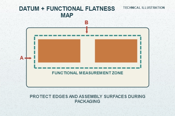
Packaging should protect ceramic edges and finished copper surfaces from impact, abrasion and contamination. State orientation, separator material and any vacuum or dry-pack requirement that follows from the finish and assembly storage plan.
How Should the Surface Finish Match Die Attach and Interconnection?
The finish decision begins with the assembly route: solder or silver sinter for die attach; aluminum wire, copper wire, ribbon or clip for top interconnection; and solder, sinter or another method at the lower interface. Each route has its own requirements for finish type, thickness, cleanliness, roughness and storage life.
When the project can use DBC instead of AMB, our automotive Ni/Pd/Au DBC ceramic substrate provides a relevant plated alternative. The route must be selected before the finish is copied from one technology to another.
What Should the Delivery Acceptance Plan Contain?
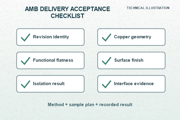
An effective plan links each critical characteristic to a method, sample plan and record.
| Characteristic | Acceptance record | Why the assembler needs it |
|---|---|---|
| Artwork and revision | Released file identifier | Prevents mixed design versions |
| Finished copper geometry | AOI and dimensional report | Protects attach and bond areas |
| Functional flatness | Defined datum and measured result | Supports controlled bond-line thickness |
| Surface finish | Process certificate or agreed measurement | Confirms joining compatibility |
| Electrical isolation | Test condition and result | Confirms the bare-substrate requirement |
| Braze/interface evidence | Agreed inspection or coupon record | Supports interface process control |
This table should be customized to the drawing. Adding reports that do not connect to a requirement increases paperwork without reducing assembly risk.
What Should Incoming Inspection Confirm Before Assembly?
At receiving, verify package integrity, part and revision identity, quantity, orientation, critical dimensions, surface condition and any required traceability labels. Do not repeat destructive interface analysis on every lot unless the control plan requires it; instead, connect supplier process evidence with a practical incoming sampling plan.
For programs that remain on DBC, our DBC ceramic substrate for IGBT semiconductors is the closer alternative to review. It should be treated as a different bonded-copper route, not as an AMB part with a changed name.
How Do We Control the Move from Prototype to Production?
We manufacture custom AMB ceramic circuits for power-module projects and review the ceramic, copper, braze construction, pattern, finish and acceptance evidence before release. For suitable designs, our published AMB route supports rapid prototyping; actual timing and volume planning are confirmed after the files and process requirements are reviewed.
Prototype deviations must become formal drawing or control-plan revisions. A change to die layout, copper thickness, surface finish, datum or joining process triggers a targeted review of the affected characteristics instead of an automatic repeat of every test.
What Should You Include in an AMB Substrate RFQ?
For our AMB substrate RFQ review, send Gerber or ODB++ data, a dimensioned drawing, ceramic grade or required properties, finished copper and ceramic thicknesses, active-braze requirements when controlled, surface finish, die map, die-attach and interconnect methods, datums, functional flatness area, isolation test, interface evidence, sample quantity and forecast volume.
Email the package to sales@bstceramicpcb.com. We will identify missing manufacturing and acceptance inputs before quotation. An AMB substrate for traction inverter becomes assembly-ready through a controlled handoff, not through the AMB label alone.
 Products
 About us
 Contact us



