






















































 HOME
HOME

-

Ceramic PCB for Humanoid Robot joint actuators
2026 04,07 -
LTCC PCB Surprises: What Most People Miss
2025 12,09 -
Step-by-Step Guide to DPC PCB Design for Sensor Systems
2025 12,03 -
Ceramic PCBs Essential Benefits and Applications
2025 12,01 -
How Al2O3 DPC Ceramic Substrate PCB Enhances Heat Dissipation in Modern Electronics?
2025 11,28 -
How to Choose Between Ceramic, FR4, and Metal Core PCBs
2025 11,27 -
DPC Ceramic PCB Materials: Surprising Science Inside
2025 11,26 -
Wire bondable 2-layer Alumina substrates PCB | Bstceramic PCB
2025 09,22 -
Silicon Nitride Substrate, Silicon Nitride Ceramic Substrate Formula
2025 05,08 -
What is thick film ceramic PCB?
2023 08,02
Choosing a Ceramic Package for Photonic ICs
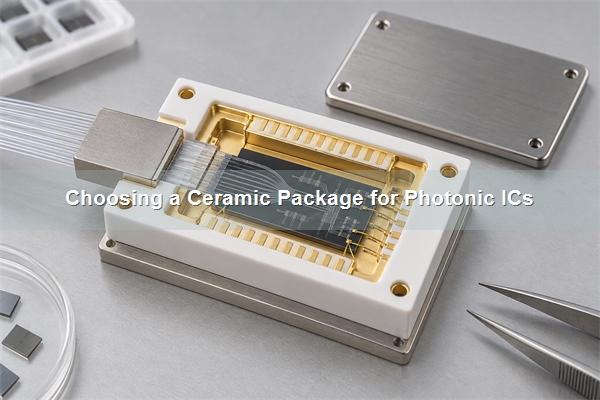
A ceramic package for photonic ICs provides a stable platform for a photonic integrated circuit (PIC), its electrical connections, optical interface and heat path. Ceramic is most useful when the assembly needs tight dimensional control, low outgassing, high electrical insulation, controlled RF feedthroughs or a hermetic cavity. It is not automatically the best choice for every optical module: the package must justify its cost by solving a defined alignment, thermal, electrical or environmental problem.
What Is a Ceramic Package for Photonic ICs?
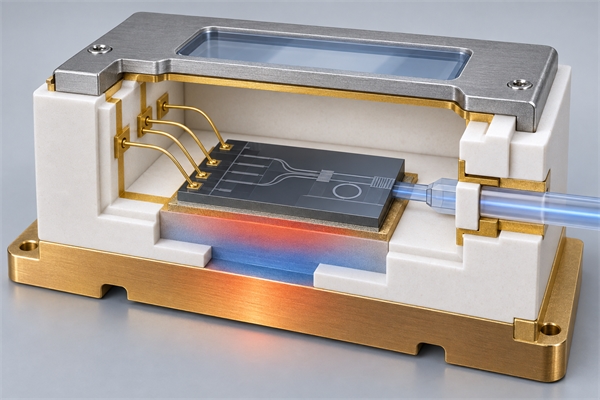
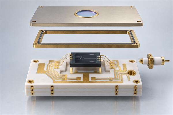
A ceramic package for photonic ICs is a ceramic-based housing, carrier or multilayer body that positions a PIC and connects it to fibers, waveguides, drivers, detectors and the next level of the electronic assembly. Depending on the architecture, it may include a cavity, patterned conductors, vias, RF or DC feedthroughs, a die-attach area, an optical window or fiber port, a heat-spreading feature and a lid.
The terms should not be mixed. A PIC is the optical semiconductor die. A ceramic substrate is the insulating circuit base. A ceramic package combines the substrate or body with electrical, thermal, mechanical and environmental interfaces. A complete photonic module may add lasers, fiber arrays, lenses, thermoelectric coolers, connectors and control electronics. This boundary matters because a ceramic circuit manufacturer may supply the metallized base or multilayer body without performing every optical alignment and final sealing operation.
What Functions Must the Package Perform?
The package must preserve optical coupling while routing electrical signals, removing heat and protecting delicate interfaces. These functions interact: a thicker heat spreader can improve temperature control but change the mechanical stack, while a new feedthrough can alter RF performance or reduce room for a fiber array.
| Package function | What must be controlled | Practical design check |
|---|---|---|
| Optical positioning | PIC, fiber, lens or waveguide position and angle | Build the complete datum and tolerance chain, including attach material and cure shift |
| Electrical connection | DC bias, control, RF launches, return paths and isolation | Model feedthroughs, wire bonds, vias and package-to-board transitions together |
| Thermal control | Junction temperature, gradients and wavelength-sensitive drift | Calculate the path from die attach through ceramic and base, not ceramic conductivity alone |
| Mechanical support | Flatness, stiffness, die stress and connector loads | Avoid over-constraining brittle ceramic or transferring fiber loads into the die area |
| Environmental protection | Moisture, particles, corrosion and outgassing | Choose hermetic or non-hermetic construction from the actual exposure and lifetime target |
Which Ceramic Materials and Structures Fit Photonic ICs?
Material selection starts with heat flux, dielectric behavior, expansion compatibility, routing density, cavity geometry and sealing method. Alumina and aluminum nitride (AlN) are ceramic compositions; HTCC and LTCC are co-fired material and manufacturing systems. They should not be treated as four interchangeable material grades.
| Option | Useful package role | Main limitation to verify |
|---|---|---|
| Alumina | Stable insulating base, cavity package or metallized carrier for moderate heat loads | Its thermal conductivity may be insufficient when a laser or driver creates concentrated heat |
| AlN | High-conductivity carrier or package base under heat-sensitive lasers, detectors and dense PIC assemblies | Material grade, metallization compatibility, handling and cost must be specified |
| HTCC | Multilayer ceramic body with buried conductors, vias, cavities and brazed metal features | Co-fired conductor system, shrinkage and achievable geometry constrain the layout |
| LTCC | Compact multilayer routing, embedded features and high-frequency package structures | Thermal conductivity, dielectric loss, conductor system and dimensional control are material-system dependent |
| Planar DPC or thin film | Fine die pads, wire-bond surfaces, compact routing and controlled top-side geometry | It does not by itself create a sealed cavity or complete optical package |
For a planar laser or PIC carrier, a DPC ceramic substrate for laser equipment illustrates the type of precise metallized ceramic circuit that can support die and connection features. Where heat must be removed through the ceramic, an AlN DPC ceramic substrate is a more relevant starting point than automatically increasing package size.
How Should Optical Alignment Be Designed?
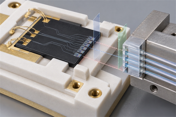
Optical alignment must be designed as a mechanical tolerance system, not left as a final assembly adjustment. The critical chain can include the PIC waveguide, die edge, die-attach thickness, package pocket, fiber array, lens, window and external connector. A small error at several interfaces can create a larger coupling loss than any single drawing tolerance suggests.
Passive alignment uses manufactured datums, stops, grooves or pockets to locate parts without continuous optical feedback. It supports scalable assembly when component and package tolerances are already tight enough. Active alignment monitors optical power while a fiber, lens or laser is positioned and fixed. It can recover coupling performance, but fixture access, adhesive cure movement, cycle time and later thermal drift must be included in the process plan.
Locate the primary optical datums near the optical interface, separate them from non-critical outer dimensions, and define the measurement condition. Flatness, cavity depth and port position should be specified at the functional surface. If the lid or window can move during sealing, the optical path must be validated after sealing rather than only before it.
How Do Thermal and Electrical Interfaces Affect Performance?
A photonic module can contain both temperature-sensitive optical elements and high-speed electronic devices. Laser wavelength, detector noise, modulator behavior and coupling stability can all move with temperature. The thermal model should include die attach, metallization, ceramic thickness, heat spreader, package base, interface material and heat sink. High ceramic thermal conductivity helps only when the ceramic is a meaningful part of the total resistance.
Electrical transitions deserve the same system view. A feedthrough that looks acceptable as an isolated trace may create a discontinuity when combined with a via, wire bond, bond pad, cavity wall and external connector. RF paths need controlled geometry and a continuous return-current path. DC lines may need isolation, current capacity and filtering without coupling noise into detectors or modulators.
For multilayer routing in demanding communication hardware, an HTCC ceramic substrate for satellite communication provides a relevant example of compact, high-reliability ceramic interconnect construction. When lower-temperature co-firing and integrated high-frequency routing are a better fit, an LTCC ceramic substrate for power-amplifier circuits shows another multilayer route. The final choice still depends on the qualified material system, frequency, loss target, via design and assembly sequence.
When Is Hermetic Sealing Necessary?
Hermetic sealing is justified when moisture, particles, reactive gases or long-term contamination can damage exposed optical surfaces, wire bonds, lasers, detectors or die-attach interfaces. It is also common when the module must survive severe temperature, pressure or storage conditions. Ceramic supports a hermetic structure, but ceramic alone does not make a package hermetic.
The complete enclosure must control leakage through the lid joint, optical window, fiber feedthrough, electrical feedthroughs and brazed interfaces. Seam-welded metal lids can limit the heat-affected area, while solder, glass and other seal systems impose different temperature and material-compatibility constraints. Leak acceptance criteria and test method must be defined for the finished enclosure.
A non-hermetic package can be the better choice when the PIC and interconnects are adequately passivated, the operating environment is controlled, and the product architecture prioritizes volume, rework or low-temperature assembly. The decision should follow a contamination and lifetime analysis rather than the assumption that hermetic is always more reliable.
Which Metallization, Bonding and Lid Processes Matter?
Metallization must match the attachment process and signal function. Wire bonding needs a compatible finish, clean pad surface and controlled pad geometry. Flip-chip assembly adds bump metallurgy, stand-off, underfill and rework constraints. Brazed leads, frames or heat spreaders introduce another high-temperature step and another coefficient-of-thermal-expansion interface.
The package process sequence should be frozen before finalizing materials. A typical sequence may include ceramic forming or substrate preparation, conductor and via formation, co-firing or plating, metal-part attachment, surface finishing, die attach, interconnect assembly, optical alignment, cleaning, lid sealing and final testing. Changing the order can expose a die or optical adhesive to a temperature it cannot tolerate.
What Common Packaging Failures Should Be Prevented?
Most failures start at an interface rather than in the ceramic bulk. The validation plan should target the interface that carries the largest optical, thermal, electrical or mechanical risk.
| Failure mode | Likely design or process cause | Useful verification |
|---|---|---|
| Optical power loss after cure or seal | Adhesive shrinkage, lid-induced movement or incomplete datum control | Measure coupling before and after cure, sealing and thermal cycling |
| Hot die or wavelength drift | Die-attach voids, an interrupted heat path or undersized heat spreader | Thermal simulation plus temperature mapping on a representative assembly |
| Ceramic crack or delamination | CTE mismatch, sharp corners, thick asymmetric metal or excessive clamp load | Cross-section, thermal cycling and mechanical-load validation |
| RF loss or resonance | Poor return path, long wire bonds, uncontrolled feedthrough or cavity coupling | EM simulation and S-parameter measurement through the assembled transition |
| Leakage or contamination | Seal void, window/feedthrough defect, residue or incompatible outgassing material | Leak test, cleanliness control and environmental aging |
| Bond lift or corrosion | Wrong finish, contamination, intermetallic growth or moisture exposure | Bond-pull or shear testing and material-specific aging |
What Should Be Defined Before Fabrication?
Fabrication should begin only after the optical, electrical, thermal and mechanical interfaces agree with one another. A package outline without datum definitions or interface conditions is not enough.
- PIC, laser, detector and driver dimensions, pad map, backside condition and allowable assembly temperature
- Optical interface type, fiber or waveguide position, coupling direction, datum scheme and allowable alignment loss
- Ceramic composition or co-fired system, layer count, finished thickness, cavity depth, flatness and critical tolerances
- Conductor and via structure, line geometry, impedance targets, current, isolation and surface finish
- Die-attach, wire-bond or flip-chip metallurgy, heat-spreader interface and intended thermal path
- Lid, window, seal ring, sealing method, internal atmosphere and leak-test requirement when applicable
- Assembly sequence, cleaning limits, rework restrictions and post-assembly inspection
- Prototype test plan covering optical coupling, thermal behavior, electrical performance and environmental reliability
At BSTCeramicPCB, we can review the ceramic circuit portion against the required material, metallization, vias, cavities, tolerances and assembly interfaces. Optical alignment, final package sealing and module-level qualification should be assigned explicitly so the drawing does not imply an unverified responsibility.
FAQ
Is a ceramic package always hermetic?
No. Hermeticity depends on the lid, seal, windows, fiber ports, feedthroughs and tested leak rate of the complete enclosure. An open ceramic substrate is not hermetic.
Is AlN always better than alumina for photonic packaging?
No. AlN is valuable when the ceramic layer limits heat removal, but alumina may be more economical and fully adequate for moderate heat loads. Compare the complete thermal resistance, metallization process and mechanical requirements.
Can a ceramic package carry both optical and RF interfaces?
Yes, but the interfaces must be co-designed. Optical datums, cavity walls, RF return paths, feedthroughs and connectors compete for space and can affect one another.
Is photonic chip packaging the same as mounting a PIC on a ceramic PCB?
No. Mounting the die on a ceramic circuit provides electrical and thermal connections, but photonic chip packaging may also require fiber or lens alignment, optical adhesives, windows, environmental protection, a lid and module-level testing.
Which tests are most important for integrated photonics packaging?
The test set should follow the failure risks. Common checks include optical insertion loss before and after thermal cycling, temperature mapping, S-parameters for high-speed transitions, bond pull or shear, die-attach inspection, leak testing for hermetic packages and environmental aging.
Conclusion
Choosing a ceramic package for photonic ICs starts with the interface that has the smallest margin: optical alignment, device temperature, RF transition, environmental protection or mechanical stability. Select alumina, AlN, HTCC, LTCC or a planar metallized ceramic only after that constraint is clear, then verify the assembled optical, thermal and electrical paths together. For a ceramic substrate and metallization review based on your package drawing, contact BSTCeramicPCB at sales@bstceramicpcb.com.
 Products
 About us
 Contact us



