






















































 HOME
HOME

-

Ceramic PCB for Humanoid Robot joint actuators
2026 04,07 -
LTCC PCB Surprises: What Most People Miss
2025 12,09 -
Step-by-Step Guide to DPC PCB Design for Sensor Systems
2025 12,03 -
Ceramic PCBs Essential Benefits and Applications
2025 12,01 -
How Al2O3 DPC Ceramic Substrate PCB Enhances Heat Dissipation in Modern Electronics?
2025 11,28 -
How to Choose Between Ceramic, FR4, and Metal Core PCBs
2025 11,27 -
DPC Ceramic PCB Materials: Surprising Science Inside
2025 11,26 -
Wire bondable 2-layer Alumina substrates PCB | Bstceramic PCB
2025 09,22 -
Silicon Nitride Substrate, Silicon Nitride Ceramic Substrate Formula
2025 05,08 -
What is thick film ceramic PCB?
2023 08,02
Ceramic PCB Applications: Industry Uses and Material Selection
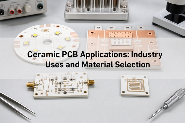
Ceramic PCB applications include power modules, LED and laser systems, RF circuits, automotive electronics, aerospace controls, medical equipment, and industrial sensors. The common requirement is not simply “high performance.” Ceramic becomes useful when the circuit substrate must transfer heat, isolate voltage, hold dimensions, or remain stable under conditions that push FR4 beyond a practical limit.
What Makes Ceramic PCBs Suitable for Demanding Applications?
Ceramic PCBs are selected when the substrate is part of the thermal, electrical, or mechanical design. Alumina, aluminum nitride, and silicon nitride are electrically insulating, yet they conduct heat more effectively than organic laminates. Their low moisture uptake and dimensional stability also help circuits retain predictable behavior across temperature changes.
| Application trigger | Why ceramic helps | What still needs engineering control |
|---|---|---|
| Concentrated heat source | Moves heat through an electrically insulating substrate | Die attach, copper spreading, interface material, and heatsink resistance |
| High voltage in limited area | Combines dielectric isolation with a short thermal path | Creepage, clearance, edge condition, metallization spacing, and contamination |
| RF or microwave signal path | Provides stable dielectric behavior and precise geometry | Material loss tangent, substrate thickness, conductor roughness, and launch design |
| Repeated temperature cycling | Offers stable inorganic material and controlled expansion | Copper balance, joint fatigue, substrate fracture toughness, and mounting stress |
| High-temperature or sealed assembly | Avoids resin softening and moisture-related laminate changes | Metallization, surface finish, solder, braze, and package limits |
Ceramic does not make the entire assembly immune to heat or stress. The weakest interface may still be a solder layer, brazed joint, wire bond, connector, or mechanical clamp.
Which Ceramic Materials Fit Different PCB Applications?
Material choice begins with the required heat path and mechanical duty. Values below are typical commercial ranges at room temperature; a project specification should use the selected supplier grade rather than a generic handbook value.
| Ceramic material | Typical thermal conductivity | Strong application fit | Main boundary |
|---|---|---|---|
| 96% alumina (Al2O3) | About 20-25 W/m-K | Sensors, hybrid circuits, medical electronics, moderate-power LEDs, heaters, and cost-controlled modules | Lower heat transfer than AlN or Si3N4 |
| High-purity alumina | Often about 25-30 W/m-K | Circuits needing improved dielectric performance, surface quality, or dimensional stability | Higher cost than standard alumina |
| Aluminum nitride (AlN) | Common grades about 140-180 W/m-K | Laser diodes, high-power LEDs, RF power devices, and compact semiconductor packages | Higher cost and more demanding process and moisture control |
| Silicon nitride (Si3N4) | Common substrate grades about 70-90 W/m-K | Traction inverters and power modules exposed to strong thermal cycling and mechanical stress | Chosen for toughness, not maximum conductivity; supply and process options are more specialized |
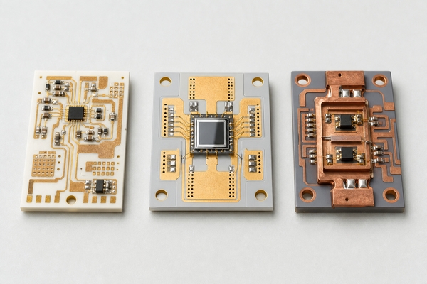
Alumina is the practical baseline when its thermal resistance meets the junction-temperature target. AlN is justified when the ceramic layer is a significant bottleneck. Si3N4 is often selected when fracture toughness and power-cycle durability carry more weight than the highest possible conductivity.
How Are Ceramic PCBs Used in Power Electronics?
Power semiconductors create high local heat while requiring electrical isolation from a baseplate or cooling structure. DBC and AMB substrates place thick copper on ceramic so the copper can carry current and spread heat laterally while the ceramic transfers heat through its thickness.
IGBT and MOSFET power modules
An IGBT or MOSFET module may use Al2O3, AlN, or Si3N4 beneath copper conductor islands. AlN reduces substrate thermal resistance, while Si3N4 improves resistance to crack growth and repeated thermomechanical loading. The best choice depends on chip heat flux, module area, copper thickness, baseplate architecture, and the required power-cycle life.
A live example is this DBC ceramic substrate for IGBT semiconductor modules. Its relevance is the combination of bonded copper, electrical isolation, and a direct heat path used in high-current power packaging.
Inverters, converters, and power supplies
Ceramic substrates can shorten the path from switching devices to the cooling surface and reduce the need for separate insulating pads. They are useful in traction inverters, industrial drives, renewable-energy converters, and compact power supplies. A thermal model should include the semiconductor junction, die attach, copper, ceramic, substrate attach, thermal interface material, and coolant path; quoting only ceramic thermal conductivity can hide the true bottleneck.
Why Are Ceramic PCBs Used in LEDs and Laser Systems?
High-power LEDs and laser diodes place a concentrated heat source close to optically sensitive structures. Junction temperature affects optical output, wavelength stability, efficiency, and lifetime. A ceramic submount provides electrical isolation while conducting heat toward a metal carrier or heatsink.
Alumina is suitable when power density is moderate and cost matters. AlN is preferred when the package footprint is small, heat flux is high, or temperature uniformity is critical. Thin film or DPC supports fine pads and wire-bond features; thick copper is useful when lateral spreading or current capacity dominates.
The alumina DPC ceramic substrate for LED modules shows how plated circuitry can combine precise component pads with a ceramic heat path. The same architecture may need AlN rather than alumina when calculations show the substrate temperature drop is too high.
Where Do Ceramic PCBs Fit in RF and Microwave Circuits?
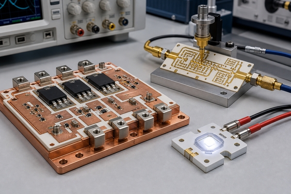
RF performance depends on more than the word “ceramic.” Dielectric constant, loss tangent, thickness tolerance, surface roughness, conductor profile, and temperature stability determine impedance and insertion loss. Thin film, DPC, and LTCC are common choices because they can support controlled geometry, fine features, or multilayer integration.
Thin film suits precision matching networks, filters, attenuators, and microwave transmission lines. DPC is useful when the design needs plated copper, vias, and more conductor thickness than a thin-film stack. LTCC can integrate buried conductors, vias, cavities, and passive structures in a compact RF package.
This thin film ceramic PCB for wireless communication is directly relevant to RF layouts where conductor definition and stable ceramic geometry matter. The final stackup still requires an impedance model based on the selected ceramic grade and finished metal thickness.
How Are Ceramic PCBs Applied in Automotive and Aerospace Electronics?
Automotive ceramic PCBs appear in traction inverters, on-board chargers, voltage and pressure sensors, LED lighting, and control modules exposed to heat. Aerospace uses include radar, satellite communication, avionics, sensor interfaces, and high-temperature instrumentation.
The shared challenge is environmental cycling. The ceramic itself may remain stable, but copper, solder, die attach, packages, and housings expand at different rates. Larger copper islands and thicker copper can raise stress near corners and edges. Balanced copper, rounded conductor features, controlled substrate thickness, compliant attachment, and validated mounting loads improve reliability.
HTCC and LTCC become attractive when the application needs multilayer routing, sealed feedthroughs, embedded passive structures, or a compact ceramic package. DBC and AMB are stronger fits when current capacity and heat spreading dominate.
Which Medical and Industrial Systems Use Ceramic PCBs?
Medical and industrial systems use ceramic circuits in imaging equipment, analytical instruments, sensor interfaces, precision heaters, motor drives, power supplies, and control electronics. Thick film technology is valuable because conductors, resistors, heaters, and dielectric layers can be printed and fired on the same substrate. Thin film is better when resistance tolerance, fine geometry, or signal precision is tighter.
The Al2O3 thick film ceramic substrate for medical devices illustrates an application where printed circuit functions and stable ceramic insulation are more important than maximum thermal conductivity.
Which Manufacturing Process Fits Each Application?
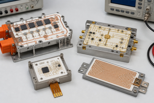
The substrate material and the metallization process are separate decisions. The same alumina plate may carry thick-film paste, thin-film metal, or plated copper, but each route has different geometry and attachment limits.
| Process | Best application fit | Key design constraint |
|---|---|---|
| Thick film | Printed resistors, heaters, sensors, hybrid circuits, and economical medium-density layouts | Paste system, firing profile, print resolution, resistance trim, and surface planarity |
| Thin film | RF, microwave, optical submounts, precision networks, and fine wire-bond pads | Substrate surface finish, film adhesion, metal thickness, and photolithographic tolerance |
| DPC | Fine copper features, plated vias, LED boards, sensors, and compact power or optoelectronic substrates | Plating uniformity, copper thickness, via geometry, adhesion, and stress |
| DBC/DCB | IGBT and MOSFET modules, inverters, converters, and high-current assemblies | Copper etching limit, copper balance, ceramic thickness, edge stress, and void control |
| AMB | High-reliability power modules, often using Si3N4 | Braze chemistry, joint quality, copper geometry, flatness, and thermal-cycle qualification |
| LTCC/HTCC | Multilayer RF modules, sensors, packages, feedthroughs, and harsh-environment electronics | Co-fire shrinkage, conductor compatibility, via registration, cavities, and process-specific rules |
The existing BST guide to ceramic circuit board process applications provides a process-by-process overview. For a new design, the application should first define heat, voltage, frequency, geometry, and lifetime targets; the manufacturing route follows from those constraints.
When Is a Ceramic PCB Unnecessary?
A ceramic PCB is usually unnecessary when FR4 already meets component temperature, voltage isolation, signal loss, and lifetime targets. FR4 is easier to route in many layers, drill, panelize, assemble, rework, and source at scale. A metal-core PCB may also be sufficient for single-sided LED or power circuits when the dielectric layer and thermal path meet requirements.
Avoid selecting AlN only because its conductivity is higher. If most thermal resistance sits in the package, solder, interface material, or heatsink, changing the substrate may produce little system-level improvement. Likewise, ceramic does not automatically improve RF performance if the selected grade, thickness tolerance, and conductor structure are poorly controlled.
What Should Be Validated Before Production?
Validation should reproduce the actual stackup and mechanical boundary conditions rather than test an isolated ceramic coupon.
- Confirm substrate material, grade, thickness, flatness, and surface condition.
- Model the full thermal path and identify the largest resistance before changing materials.
- Define conductor technology, finished thickness, minimum feature sizes, and current density.
- Check creepage, clearance, dielectric strength, and edge quality at the working voltage.
- Review copper balance, corner geometry, holes, slots, and mounting loads for crack risk.
- Match surface finish to soldering, brazing, die attach, wire bonding, or conductive adhesive.
- Use thermal cycling or power cycling that represents the operating temperature range and ramp rate.
- Inspect metallization adhesion, voids, warpage, edge chips, electrical continuity, and dimensional tolerance.
A ceramic PCB prototype is most useful when it preserves the production substrate grade, copper or film construction, attachment materials, and test conditions. A visually similar prototype with a different metallization stack may not predict production reliability.
Ceramic PCB Applications FAQ
What are the most common ceramic PCB applications?
The most common uses are power modules, high-power LEDs, laser diode submounts, RF and microwave circuits, automotive power electronics, aerospace controls, medical equipment, sensors, and industrial heaters.
Which ceramic is best for high-power electronics?
AlN is strong when low substrate thermal resistance is the priority. Si3N4 is often better when fracture toughness and thermal-cycle durability are critical. Alumina remains practical for moderate power and cost-controlled designs.
Are ceramic PCBs only used for heat dissipation?
No. They are also used for electrical isolation, stable dielectric behavior, precise dimensions, high-temperature operation, printed resistors or heaters, bare-die attachment, wire bonding, and multilayer ceramic packaging.
Can ceramic PCBs replace FR4 in every application?
No. FR4 is usually better for large multilayer boards, dense conventional routing, connectors, mechanical flexibility, easy rework, and cost-sensitive products whose thermal and environmental limits are already satisfied.
What is the difference between DBC and DPC applications?
DBC favors thick bonded copper, high current, and power-module heat spreading. DPC favors plated copper, finer features, vias, and compact LED, sensor, or optoelectronic layouts. Finished geometry and reliability targets should decide between them.
How should a ceramic PCB be mounted?
The mounting method should avoid point loads and board bending. Flat support, controlled fastener torque, compliant interface materials, suitable edge clearance, and attention to housing flatness reduce crack risk.
Conclusion
Ceramic PCB applications make sense when the substrate must provide a defined thermal path, electrical isolation, RF stability, or environmental durability that FR4 cannot provide efficiently. Material conductivity is only one part of the decision; copper geometry, metallization, interfaces, mounting, and lifetime testing determine whether the finished assembly performs reliably.
BSTCeramicPCB can review the ceramic material, metallization route, copper or film construction, and test conditions for application-specific ceramic circuits. For technical communication about an existing design, contact sales@bstceramicpcb.com.
 Products
 About us
 Contact us



