






















































 HOME
HOME


-

Ceramic PCB for Humanoid Robot joint actuators
2026 04,07 -
LTCC PCB Surprises: What Most People Miss
2025 12,09 -
Step-by-Step Guide to DPC PCB Design for Sensor Systems
2025 12,03 -
Ceramic PCBs Essential Benefits and Applications
2025 12,01 -
How Al2O3 DPC Ceramic Substrate PCB Enhances Heat Dissipation in Modern Electronics?
2025 11,28 -
How to Choose Between Ceramic, FR4, and Metal Core PCBs
2025 11,27 -
DPC Ceramic PCB Materials: Surprising Science Inside
2025 11,26 -
Wire bondable 2-layer Alumina substrates PCB | Bstceramic PCB
2025 09,22 -
Silicon Nitride Substrate, Silicon Nitride Ceramic Substrate Formula
2025 05,08 -
What is thick film ceramic PCB?
2023 08,02
Ceramic PCB Copper Thickness Guide: DPC, DBC and AMB Selection
Published:
A ceramic PCB copper thickness guide helps engineers choose copper that can carry current, spread heat and still meet the line width, spacing and bonding limits of the selected ceramic process. For ceramic PCBs, copper thickness is not only a conductivity value. It affects etching accuracy, thermal stress, soldering behavior, surface finish choice, cost and whether DPC, DBC or AMB is the right manufacturing route.
In practical sourcing, the best copper thickness is usually the thinnest copper that can meet current, temperature rise, thermal spreading and reliability targets with enough manufacturing margin. A fine-line sensor board may need plated DPC copper, while an IGBT or SiC power module may need much thicker copper on DBC or AMB ceramic substrate.
What Does Copper Thickness Mean in Ceramic PCB Design?
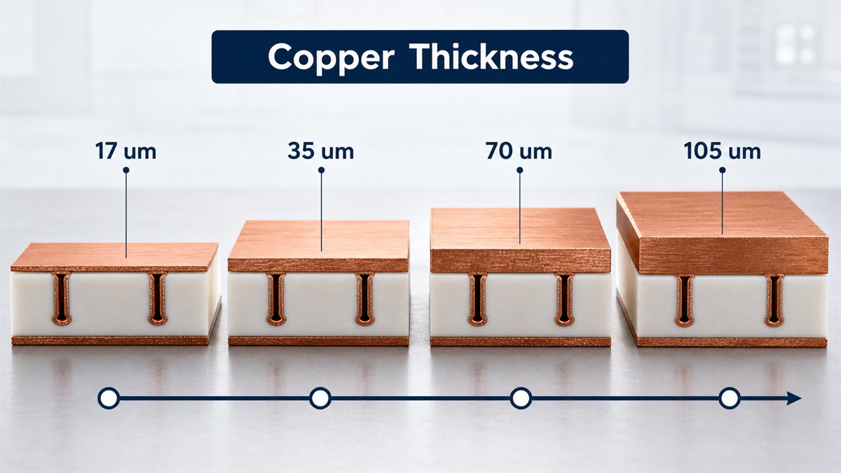
Copper thickness means the finished conductive copper on the ceramic surface, usually specified in micrometers, millimeters or copper weight. A conventional PCB often uses ounce-based copper weights, where 1 oz copper is commonly treated as about 35 micrometers. Ceramic power substrates may also use much thicker copper, especially when the copper layer is bonded as foil rather than built only by plating.
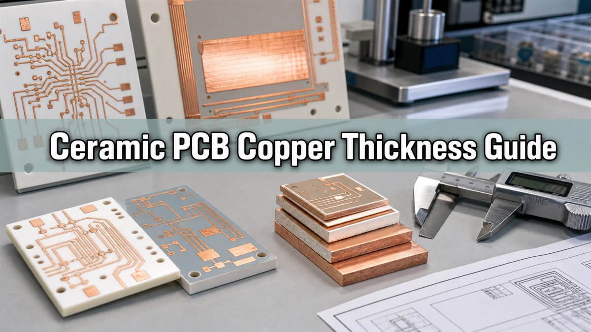
The buyer should confirm whether the supplier is quoting base copper, finished copper or plated copper after patterning. This matters because a drawing that simply says "2 oz copper" can be clear for a standard PCB but incomplete for a ceramic substrate if the process route, ceramic thickness, copper symmetry and surface finish are not defined.
| Copper specification | Approximate thickness | Typical use in ceramic PCB discussion |
| 0.5 oz | About 17 micrometers | Fine signals, low current, thin plated structures |
| 1 oz | About 35 micrometers | General routing, moderate current, easier etching |
| 2 oz | About 70 micrometers | Higher current, wider traces, more thermal spreading |
| 3 oz | About 105 micrometers | Heavy copper routing where spacing and etching margin allow it |
| 0.2-0.5 mm copper | 200-500 micrometers | Commonly discussed for DBC or AMB power substrate designs |
How Does Copper Thickness Change by Ceramic PCB Process?
Copper thickness depends strongly on the ceramic PCB technology because DPC, DBC, AMB and thick-film ceramic circuits form copper or conductor layers in different ways. The process route should be selected before the final copper thickness is locked.
| Process | Copper or conductor approach | Best fit | Design caution |
| DPC ceramic PCB | Seed layer plus electroplated copper | Fine lines, vias, compact LED, sensor and module circuits | Very thick copper can reduce fine-line capability and increase plating time |
| DBC/DCB ceramic substrate | Copper foil directly bonded to ceramic | Power modules, inverters, heat spreaders and high-current paths | Thicker copper needs wider spacing and careful stress management |
| AMB ceramic substrate | Copper foil brazed to ceramic with active metal filler | SiC modules, IGBT modules and high thermal cycling applications | Material, copper symmetry and bonding reliability must be reviewed together |
| Thick-film ceramic circuit | Screen-printed conductor paste fired on ceramic | Hybrid circuits, sensors, resistive networks and compact functional modules | Do not compare printed conductor thickness directly with bonded copper foil |
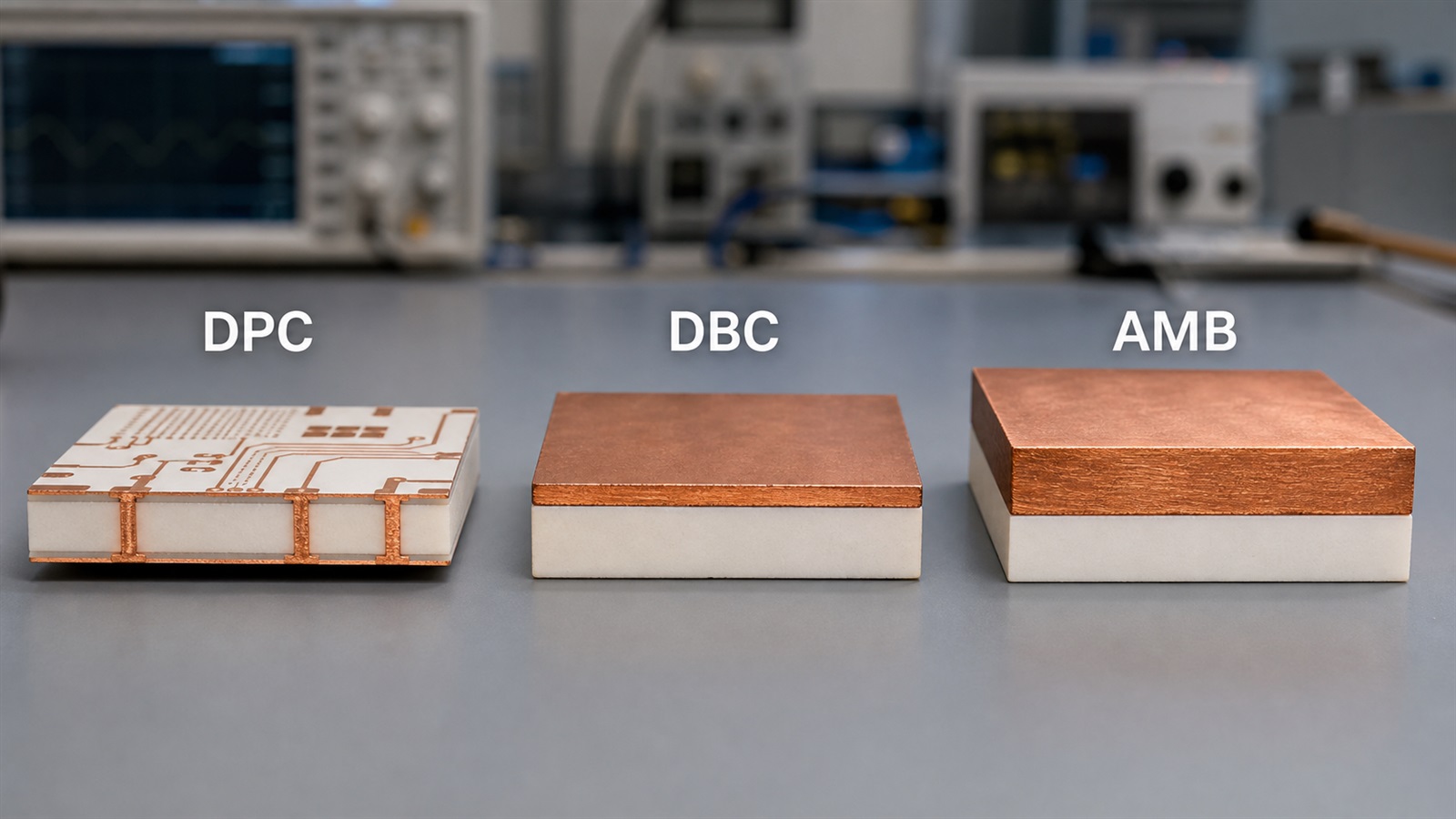
For example, a compact optical board may start with a DPC ceramic substrate PCB because routing density matters. A traction inverter or power semiconductor base may start with a DBC ceramic board for automotive components because heat spreading and current capacity are more important than fine traces.
How Does Copper Thickness Affect Current, Heat and Line Width?
Thicker copper lowers conductor resistance and improves lateral heat spreading, but it also makes etching, spacing control and stress balance more difficult. A thicker copper layer is not automatically better if the layout needs narrow gaps, small pads or tight isolation distance.
Current capacity should be checked with trace width, allowed temperature rise, copper thickness, ambient temperature, ceramic material and cooling method. Thermal performance should be checked with the full heat path: chip attach, copper, ceramic, solder layer, baseplate, thermal interface material and heat sink. Copper thickness helps, but it cannot compensate for a poor mounting surface or an undersized heat sink.
Line width and spacing usually become more conservative as copper becomes thicker. Heavy copper requires more etching allowance, and the sidewall profile can affect the actual isolation gap. If the project needs both high current and fine spacing, the supplier should review whether the design should split power and signal functions, use a different ceramic process or adjust the copper distribution.
How Should You Choose Copper Thickness for DPC, DBC and AMB?
Choose DPC when the circuit needs fine features and moderate copper, choose DBC when the design needs thick bonded copper for heat and current, and choose AMB when the power module needs stronger copper-to-ceramic bonding under demanding thermal cycling. The copper thickness should follow that process decision, not the other way around.
| Design requirement | Recommended direction | Reason |
| Fine traces, dense pads, plated vias | DPC with moderate copper | Better routing freedom and finer pattern control |
| High current and strong heat spreading | DBC with thicker bonded copper | Bonded copper foil supports power substrate structures |
| Severe power cycling or SiC module stress | AMB with suitable copper symmetry | AMB is often selected for stronger reliability demands |
| Cost-sensitive moderate thermal design | Al2O3 ceramic with practical copper thickness | Alumina can be cost-effective when thermal margin is enough |
| High thermal conductivity requirement | AlN or Si3N4 with reviewed copper thickness | The ceramic material and copper stress must be matched |
If the requirement is uncertain, compare the article on DPC vs DBC vs AMB before locking the copper thickness. It is common for an RFQ to change after the thermal model, isolation distance and mechanical mounting method are reviewed together.
What Manufacturing Limits Should Be Checked Before Quotation?
The main manufacturing checks are finished copper thickness, minimum line width and spacing, copper-to-edge distance, ceramic thickness, surface finish, flatness, warpage and copper symmetry. These checks determine whether the design is easy to manufacture or likely to need layout changes before prototype release.
- Define finished copper thickness on each side instead of using a vague "heavy copper" note.
- Confirm minimum line width and spacing for the selected copper thickness and process.
- Check whether the copper pattern is balanced enough to reduce warpage and stress.
- Specify ceramic material, such as Al2O3, AlN or Si3N4, because thermal and mechanical behavior changes.
- State the surface finish, soldering process and assembly temperature.
- Ask whether prototype tooling, etching compensation or laser processing will affect lead time.
For power applications, an AMB ceramic PCB may need earlier review of copper thickness, ceramic fracture risk and module mounting conditions. A drawing that works electrically can still fail mechanically if copper stress, ceramic thickness and thermal cycling are ignored.
What Files Should You Send for a Copper Thickness Review?
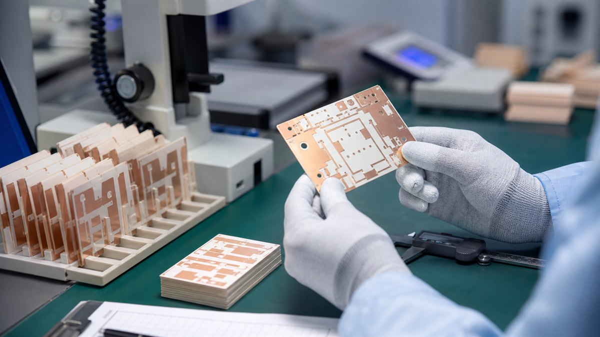
A supplier can review copper thickness more accurately when the RFQ includes layout data, stackup intent, current path, heat source, operating temperature and production quantity. Sending only a PDF image often causes quotation gaps because the fabricator cannot verify copper spacing, pad geometry or finished dimensions.
- Gerber, ODB++ or CAD data with copper layers and outline.
- Stackup note showing ceramic material, ceramic thickness and copper thickness per side.
- Current, voltage, power loss and allowed temperature rise for key nets.
- Assembly information, including soldering method, components and surface finish.
- Mechanical requirements such as mounting holes, flatness, edge clearance and heat sink interface.
- Prototype quantity, target mass production volume and inspection expectations.
BSTCeramicPCB can review copper thickness together with ceramic material and process choice for ceramic PCB projects. If the application is still in design, it is better to share the thermal target and current path before forcing a fixed copper value.
FAQ
1. What is the common copper thickness for ceramic PCB?
Common copper thickness depends on process. DPC designs often use plated copper suitable for fine circuits, while DBC and AMB substrates often use much thicker bonded copper for power modules. The drawing should state finished copper thickness in micrometers or millimeters.
2. Is thicker copper always better for ceramic PCB?
No. Thicker copper can improve current capacity and heat spreading, but it may require wider spacing, increase stress and limit fine patterning. The best choice balances electrical, thermal and manufacturing needs.
3. How thick is 1 oz copper?
One ounce copper is commonly treated as about 35 micrometers. This conversion is useful for PCB discussions, but ceramic power substrates may also specify copper directly in micrometers or millimeters.
4. Which is better for thick copper, DBC or DPC?
DBC is usually the stronger starting point for thick bonded copper and high-current power substrates. DPC is better when fine circuits, plated vias and compact routing are more important than very thick copper.
5. When should AMB be considered?
AMB should be considered when the module faces high power density, severe thermal cycling or reliability targets that justify stronger copper-to-ceramic bonding. It should be selected based on measurable stress and qualification needs.
6. Does ceramic material affect copper thickness?
Yes. Al2O3, AlN and Si3N4 have different thermal conductivity, mechanical strength and thermal expansion behavior. Copper thickness should be reviewed together with ceramic thickness and material, especially for power modules.
7. Can a ceramic PCB use different copper thickness on two sides?
It may be possible, but the design needs stress and warpage review. Symmetrical copper can be easier to control, while asymmetric copper may be needed for specific electrical or thermal functions.
8. What copper thickness should I choose for LED ceramic PCB?
For LED ceramic PCBs, choose copper based on drive current, heat density, pad size, line width and assembly method. Many LED designs need enough copper for heat spreading without sacrificing pad accuracy.
9. What information does a supplier need to quote heavy copper ceramic PCB?
The supplier needs layout files, ceramic material, ceramic thickness, finished copper thickness, minimum line spacing, surface finish, electrical load, thermal target, quantity and inspection requirements.
10. Can BSTCeramicPCB help choose copper thickness?
Yes. BSTCeramicPCB can review the copper thickness, ceramic material, process route and quotation inputs for custom ceramic PCB projects when the drawing, electrical load and application conditions are provided.
Conclusion
A practical ceramic PCB copper thickness guide should not stop at copper weight conversion. The right choice depends on the process route, current path, heat load, line width, ceramic material, bonding reliability and prototype risk. DPC is useful for fine plated ceramic circuits, DBC supports many thick-copper power substrates, and AMB becomes important when thermal cycling and module reliability are the main concerns.
If you are preparing a ceramic PCB, DPC, DBC or AMB substrate RFQ, send your files, copper thickness target, ceramic material, current load, heat conditions and quantity plan to BSTCeramicPCB. For engineering review and quotation guidance, contact sales@bstceramicpcb.com or use the contact BSTCeramicPCB page.
 Products
 About us
 Contact us



