






















































 HOME
HOME

-

Ceramic PCB for Humanoid Robot joint actuators
2026 04,07 -
LTCC PCB Surprises: What Most People Miss
2025 12,09 -
Step-by-Step Guide to DPC PCB Design for Sensor Systems
2025 12,03 -
Ceramic PCBs Essential Benefits and Applications
2025 12,01 -
How Al2O3 DPC Ceramic Substrate PCB Enhances Heat Dissipation in Modern Electronics?
2025 11,28 -
How to Choose Between Ceramic, FR4, and Metal Core PCBs
2025 11,27 -
DPC Ceramic PCB Materials: Surprising Science Inside
2025 11,26 -
Wire bondable 2-layer Alumina substrates PCB | Bstceramic PCB
2025 09,22 -
Silicon Nitride Substrate, Silicon Nitride Ceramic Substrate Formula
2025 05,08 -
What is thick film ceramic PCB?
2023 08,02
Ceramic PCB Definition: Materials, Structure and Applications
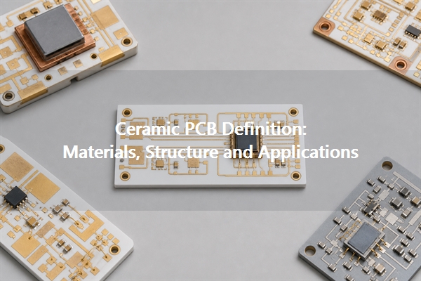
A ceramic PCB definition is a printed circuit board in which the electrically insulating base is a fired ceramic rather than an organic glass-epoxy laminate. Conductive patterns, pads, and sometimes vias are formed on or within that ceramic by thick film, thin film, direct plated copper, direct bonded copper, active metal brazing, or co-firing. The result is useful when heat flow, electrical isolation, dimensional stability, or operating temperature exceeds the practical limits of FR4.
What Is the Ceramic PCB Definition?
A ceramic PCB is an interconnection structure built on a ceramic dielectric substrate. It becomes a PCB when it contains a defined conductive network for electrical connection, not merely because a ceramic plate is present. A finished board may include metal traces, component pads, vias, resistors, dielectric layers, surface finishes, and attached components.
The term describes the substrate family, not one fixed construction. A single-sided alumina thick film circuit, a copper-clad AlN DBC substrate, a fine-line DPC board, and a multilayer LTCC module can all be ceramic PCBs, although their metal systems, current capacity, feature sizes, and manufacturing sequences differ.
How Is a Ceramic PCB Structured?
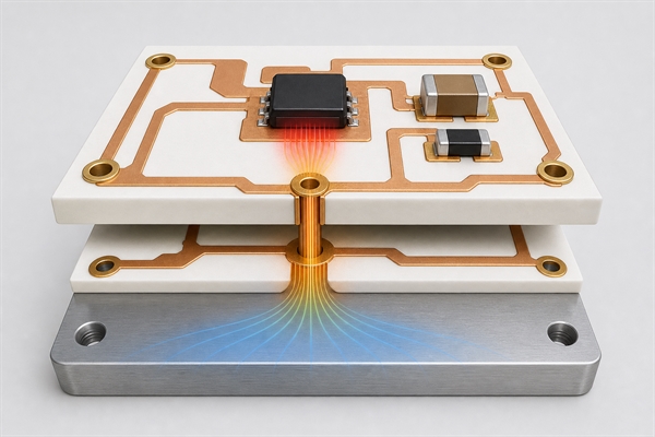
The basic structure has a ceramic dielectric supporting a patterned conductor. The conductor carries current and spreads heat laterally, while the ceramic isolates the circuit electrically and transfers heat toward a baseplate, housing, or heatsink. Surface finishes are selected for soldering, wire bonding, brazing, die attach, or corrosion control.
| Layer or feature | Function | Engineering consequence |
|---|---|---|
| Ceramic substrate | Electrical insulation, mechanical support, and through-thickness heat transfer | Material grade, thickness, flatness, and surface condition affect thermal and assembly performance |
| Metal circuit | Traces, pads, current paths, and lateral heat spreading | Metallization method controls line width, copper thickness, adhesion, and current capacity |
| Vias or filled holes | Connect front and back circuits or internal layers | Hole geometry and fill material must be compatible with ceramic processing and thermal cycling |
| Surface finish | Provides an attachment or bonding interface | Solder, wire, die-attach, and storage requirements determine the finish |
| Components and joints | Complete the electrical function | Package CTE, solder thickness, die attach, and mounting stress influence reliability |
How Does a Ceramic PCB Differ from a Ceramic Substrate?
A ceramic substrate is the insulating base material; a ceramic PCB is the functional circuit formed on or inside that base. A laser-cut alumina plate with no electrical pattern is a substrate. After metallization creates traces and pads, and the required holes, finish, and inspection are completed, it can serve as a ceramic printed circuit board.
This distinction matters in specifications. "Alumina substrate, 0.635 mm" defines only material and thickness. It does not define conductor material, copper or paste thickness, line width, via construction, surface finish, flatness, edge quality, or electrical test. Those features determine whether the item is a usable circuit rather than a ceramic blank.
Which Ceramic PCB Materials Are Common?
Material selection starts with the required heat path and mechanical loading, then considers dielectric behavior, processing compatibility, size, and cost. Thermal-conductivity values below are common room-temperature ranges, not guaranteed values for every grade or finished board.
| Material | Typical thermal conductivity | Best fit | Main limitation |
|---|---|---|---|
| 96% alumina (Al2O3) | About 20-25 W/m-K | General ceramic circuits, sensors, hybrids, LEDs, and cost-controlled designs | Lower heat transfer than AlN or Si3N4 |
| High-purity alumina | Often about 25-30 W/m-K | Applications needing improved dielectric performance or surface quality | Higher cost than standard 96% alumina |
| Aluminum nitride (AlN) | Common commercial grades about 140-180 W/m-K | Power semiconductors, laser diodes, high-power LEDs, and concentrated heat sources | Higher material and process cost; moisture and processing controls are more demanding |
| Silicon nitride (Si3N4) | Common substrate grades about 70-90 W/m-K | Power modules exposed to strong thermal cycling and mechanical stress | Higher cost and fewer general-purpose process options than alumina |
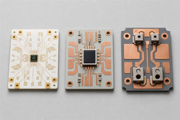
Alumina is the practical default when its heat-transfer capability is sufficient. AlN is justified when the substrate itself is a major thermal bottleneck. Si3N4 is valuable when fracture resistance and thermal-cycle durability matter as much as conductivity. A higher material conductivity does not remove the thermal resistance of solder, die attach, copper, interface material, or the heatsink.
Which Ceramic PCB Manufacturing Methods Are Used?
The manufacturing route determines conductor thickness, feature resolution, layer capability, attachment compatibility, and cost. These methods are not ceramic materials; the same alumina or AlN grade may support more than one route.
| Method | How the circuit is formed | Typical strength | Selection boundary |
|---|---|---|---|
| Thick film | Conductive, resistive, or dielectric pastes are screen-printed and fired | Printed resistors, heaters, sensors, and economical hybrid circuits | Print and firing behavior limit fine geometry and tolerance |
| Thin film | Metal is vacuum-deposited and patterned photolithographically | Fine lines, precision networks, RF, microwave, and optical submounts | Higher process cost and strict surface requirements |
| DPC | A seed layer is deposited, patterned, and built up by copper plating | Fine copper features, vias, and controlled conductor build | Copper thickness, plating uniformity, and adhesion need qualification |
| DBC or DCB | Copper foil is directly bonded to alumina or AlN at high temperature | Thick copper, high current, and strong lateral heat spreading | Fine etching is limited and thick copper increases thermal-mechanical stress |
| AMB | An active-metal braze joins copper to ceramic | Power modules requiring strong copper-to-ceramic attachment, often with Si3N4 | Braze chemistry, voids, copper balance, and thermal cycling require control |
| LTCC or HTCC | Unfired ceramic tapes, vias, and conductors are stacked and co-fired | Multilayer routing, embedded passives, cavities, and compact packages | Shrinkage, conductor compatibility, tooling, and design rules are process-specific |
Current product examples show the practical differences between these routes: a DPC ceramic PCB for new-energy vehicle electronics supports plated fine-feature circuitry, a DBC/DCB ceramic substrate for a portable cooling device uses bonded copper for heat and current, and a thick film ceramic PCB for scientific equipment demonstrates fired-paste circuitry. The application does not select the process by itself; conductor thickness, geometry, attachment, and reliability targets do.
How Does a Ceramic PCB Compare with FR4?
The decision is not whether ceramic is universally better. It is whether the application needs a ceramic property strongly enough to accept greater material cost, tighter process constraints, and brittle handling.
| Decision factor | Ceramic PCB | FR4 PCB |
|---|---|---|
| Through-substrate heat transfer | Much higher, especially with AlN | Low through the laminate; thermal vias and metal structures are often required |
| Electrical insulation | High dielectric strength with stable inorganic material | Suitable for most standard electronics when creepage, clearance, and laminate grade are correct |
| Operating temperature | Substrate remains stable at temperatures beyond organic laminates, although metal and joints still set system limits | Limited by Tg, decomposition, resin aging, and copper-laminate reliability |
| Mechanical behavior | Rigid, dimensionally stable, and brittle | Tougher and easier to panelize, drill, assemble, and rework |
| Routing density | Depends strongly on thin film, DPC, thick film, or co-fired process | Mature low-cost multilayer routing and fine drilling options |
| Cost and scale | Higher material, machining, and process-control cost | Usually lower cost with a broad global supply base |
FR4 remains the better choice when conventional multilayer routing, connectors, rework, large panel size, and low cost dominate and the thermal design already meets temperature limits. Ceramic becomes compelling when the substrate is part of the heat path, insulation barrier, precision package, or high-temperature environment.
What Are the Advantages and Limitations of Ceramic PCBs?
The main advantages are high thermal conductivity relative to organic laminates, strong electrical insulation, low moisture uptake, dimensional stability, and compatible expansion with many semiconductor and power-module structures. These properties can reduce the number of thermal interfaces and support compact high-power assemblies.
The limitations are equally important. Ceramic is brittle, so edge chips, holes, slots, screw loads, board flex, and handling impacts can cause cracks. Copper and ceramic expand at different rates, making copper balance, thickness, feature geometry, and thermal cycling important. Large or highly irregular outlines cost more to process, and rework is less forgiving than on FR4.
Where Are Ceramic PCBs Used?
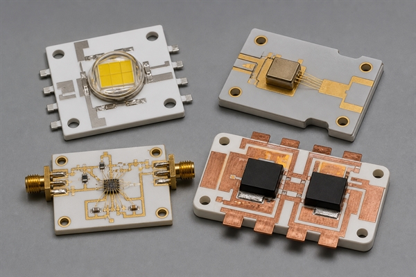
Ceramic PCBs are used when the board must do more than route signals:
- High-power LEDs and laser diodes: the substrate moves heat away from a small optical junction while maintaining electrical isolation.
- IGBT, MOSFET, and power modules: DBC, AMB, or DPC structures combine insulated heat transfer with high-current copper paths.
- RF and microwave circuits: low-loss ceramic and stable dimensions support repeatable transmission-line geometry.
- Automotive power and sensors: ceramic tolerates temperature cycling and harsh environments better than many organic laminates.
- Medical and industrial electronics: stable dielectric behavior, compact hybrid integration, and high-temperature capability support sensors, heaters, and control modules.
- Semiconductor and optoelectronic packages: ceramic submounts provide die attachment, wire-bond pads, electrical isolation, and a controlled thermal path.
When Should You Choose a Ceramic PCB?
Choose ceramic when a thermal model shows that the dielectric layer is a meaningful part of junction-to-case resistance, when the board must isolate high voltage while conducting heat, or when temperature and dimensional stability exceed FR4 capability. It is also appropriate for bare-die attachment, wire bonding, printed heaters, precision resistors, or compact power modules built around a ceramic platform.
Do not select ceramic from thermal-conductivity data alone. If the dominant resistance is the package, solder layer, thermal interface material, or heatsink, changing the PCB substrate may deliver little improvement. FR4, insulated metal substrate, heavy copper, or a metal-core PCB can be more economical when their temperature, voltage, geometry, and lifetime limits are adequate.
Which Ceramic PCB Design Limits Matter?
- Metal thickness and balance: thick or asymmetric copper creates stress and warpage during temperature change. Match copper architecture to the ceramic thickness and module size.
- Edge and hole clearance: keep metal, vias, and loaded features away from cut edges, notches, and mounting holes according to the qualified process.
- Feature rules: line width, spacing, via diameter, annular ring, and layer registration differ among thick film, thin film, DPC, DBC, and co-fired processes.
- Mechanical mounting: avoid board flex and point loads. Use controlled clamp force, compliant interfaces, washers, or supported mounting where the assembly applies pressure.
- Attachment materials: solder, braze, sintered silver, conductive adhesive, and wire bonds impose different surface-finish and temperature requirements.
- Thermal cycling: validate the complete stack, including die, copper, ceramic, joints, baseplate, and housing. Material data alone cannot predict assembly life.
- Flatness and surface quality: die attach, optical alignment, and large thermal interfaces may need tighter controls than ordinary component assembly.
Ceramic PCB Definition FAQ
Is a ceramic PCB the same as a ceramic substrate?
No. The substrate is the insulating ceramic base. A ceramic PCB includes the designed metal circuit and may also include vias, finishes, resistors, dielectric layers, and components.
What does ceramic board mean?
"Ceramic board" is an informal term that may mean a bare ceramic plate or a metallized circuit board. Drawings should state whether the requirement is an unmetalized substrate, a patterned ceramic PCB, or an assembled module.
Is a ceramic PCB electrically conductive?
The ceramic itself is electrically insulating. The patterned copper, gold, silver, or other metallization provides the conductive paths.
Can ceramic PCBs have multiple layers?
Yes. LTCC and HTCC can co-fire multilayer structures with internal conductors and vias. Other ceramic processes can create double-sided circuits and filled vias, but their stack and registration rules differ from laminated FR4 multilayers.
Is alumina or aluminum nitride better for a ceramic PCB?
Alumina is usually the cost-effective default. Aluminum nitride is better when substantially higher substrate thermal conductivity is necessary and the added material and process controls are justified.
Are DPC and DBC ceramic materials?
No. DPC and DBC are metallization technologies. Alumina, aluminum nitride, and silicon nitride are ceramic substrate materials.
Can a ceramic PCB replace FR4 directly?
Usually not without redesign. The two platforms have different thickness options, copper structures, via processes, mechanical behavior, panel formats, assembly constraints, and cost.
Why are ceramic PCBs more expensive?
The cost comes from ceramic raw material, precision firing or machining, metallization, lower panel utilization, tighter handling, and application-specific inspection. AlN, thin film, AMB, and fine-feature DPC add further process cost.
Conclusion
A practical ceramic PCB definition includes both the ceramic dielectric and the conductive circuit built on or within it. Material choice controls the thermal and mechanical foundation; thick film, thin film, DPC, DBC/DCB, AMB, or co-firing controls the circuit structure. The correct choice follows the heat path, voltage isolation, current, geometry, attachment method, and thermal-cycle requirement. For technical support with a ceramic PCB application, contact BSTCeramicPCB at sales@bstceramicpcb.com.
 Products
 About us
 Contact us



