






















































 HOME
HOME


-

Ceramic PCB for Humanoid Robot joint actuators
2026 04,07 -
LTCC PCB Surprises: What Most People Miss
2025 12,09 -
Step-by-Step Guide to DPC PCB Design for Sensor Systems
2025 12,03 -
Ceramic PCBs Essential Benefits and Applications
2025 12,01 -
How Al2O3 DPC Ceramic Substrate PCB Enhances Heat Dissipation in Modern Electronics?
2025 11,28 -
How to Choose Between Ceramic, FR4, and Metal Core PCBs
2025 11,27 -
DPC Ceramic PCB Materials: Surprising Science Inside
2025 11,26 -
Wire bondable 2-layer Alumina substrates PCB | Bstceramic PCB
2025 09,22 -
Silicon Nitride Substrate, Silicon Nitride Ceramic Substrate Formula
2025 05,08 -
What is thick film ceramic PCB?
2023 08,02
Ceramic PCB Design Guidelines: Rules, Materials, Vias and Prototype Checks
Published:
Ceramic PCB design guidelines help engineers turn a thermal, high-voltage, RF, LED, sensor, or power electronics concept into a manufacturable ceramic circuit board. The main design work is choosing the right ceramic material and process, then checking copper layout, vias, pads, edge clearance, thermal path, tolerances, and prototype files before the RFQ is sent.
What Are Ceramic PCB Design Guidelines?
Ceramic PCB design guidelines are the material, layout, thermal, mechanical, and DFM rules used to design a ceramic pcb board that can be manufactured reliably. They are different from generic FR4 PCB guidelines because ceramic substrates are harder, more brittle, more thermally conductive, and processed through different metallization and firing or bonding methods.
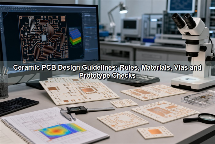
The practical goal is to reduce design changes after quotation. A ceramic PCB may look simple in a 2D Gerber file, but manufacturability depends on substrate material, copper thickness, via method, laser cutting, slot geometry, solder pad shape, thermal path, and whether the selected process is DPC, DBC, thick film, thin film, or another ceramic metallization route.
How Is Ceramic PCB Design Different from FR4 PCB Design?
Ceramic PCB design is different because the substrate itself carries the thermal and mechanical risk. FR4 is easier to drill, route, laminate, and panelize, while ceramic boards require tighter review of edge strength, brittle fracture risk, metallization adhesion, thermal expansion mismatch, and process-specific copper geometry.
| Design Area | FR4 PCB Design | Ceramic PCB Design | Engineering Note |
| Substrate role | Electrical insulation and mechanical support | Electrical insulation, thermal path, and dimensional stability | Material choice affects both circuit and heat performance |
| Mechanical processing | Drilling and routing are common | Laser cutting, punching, grinding, or controlled machining may apply | Slots and sharp corners need early DFM review |
| Copper design | Many standard copper and plating options | Depends strongly on DPC, DBC, thick film, or thin film process | Do not assume FR4 trace and spacing rules transfer directly |
| Thermal behavior | Often needs vias, copper planes, or heat sinks | Ceramic substrate may be the main heat-transfer path | Thermal pad size and heat-spreading copper matter early |
| Prototype risk | Design changes are usually easier | Material/process mismatch can delay prototype approval | Send stackup and material requirements with Gerbers |
For buyers moving from FR4, the safest first step is not to copy an old board outline. Confirm which functions require ceramic: heat transfer, high insulation, high temperature, RF stability, miniaturization, or CTE matching. If those functions are not critical, a lower-cost board type may be enough.
Which Ceramic PCB Material Should You Choose?
The material should be chosen from the electrical, thermal, mechanical, and cost needs of the application. Alumina is widely used for balanced cost and insulation, AlN is selected when high thermal conductivity is important, Si3N4 is considered where fracture toughness and power cycling matter, and BeO requires careful safety and supplier review because of handling concerns.
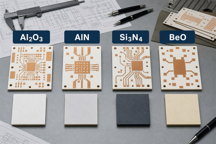
| Material | Typical Strength | Limitation | Best Fit |
| Al2O3 alumina | Cost-effective, stable insulation, mature supply | Lower thermal conductivity than AlN | LED modules, sensors, hybrid circuits, general ceramic PCB boards |
| AlN aluminum nitride | High thermal conductivity and good insulation | Higher cost and more demanding processing | Power modules, laser drivers, high-heat electronic assemblies |
| Si3N4 silicon nitride | Strong mechanical toughness and power cycling resistance | May not fit all fine-circuit or low-cost designs | High-reliability power substrates and harsh thermal cycling designs |
| BeO beryllium oxide | Very high thermal conductivity | Safety, handling, and supply-chain restrictions | Specialized thermal applications after supplier confirmation |
BSTCeramicPCB can discuss ceramic PCB material selection during quotation, but the most useful RFQ should already state the target substrate, thickness, copper thickness, operating temperature, voltage requirement, and whether the board is intended for prototype testing or production release.
What Ceramic PCB Design Rules Affect Manufacturability?
The most important ceramic pcb design rules are minimum trace and spacing, copper thickness, pad size, via method, edge clearance, slot and corner radius, board thickness, substrate size, surface finish, and process route. Exact limits are supplier-specific, so the article should treat these as DFM review categories rather than universal numbers.
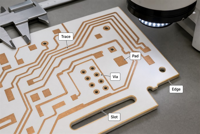
- Confirm the process first: DPC, DBC/DCB, thick film, and thin film do not share one fixed design window.
- Avoid sharp internal corners on ceramic outlines or slots where stress can concentrate.
- Keep copper features away from edges unless the supplier confirms the edge metallization design.
- Use larger pads when heavy copper, wire bonding, solder attach, or thermal cycling creates extra stress.
- Mark critical impedance, high-voltage spacing, and isolation areas clearly in the drawing.
For high-voltage or high-reliability designs, circuit board design standards such as IPC design references can help organize documentation and quality expectations, but ceramic PCB manufacturability still depends on the supplier's material and process capability. Do not rely on a generic standard table without a ceramic DFM review.
How Should Vias, Pads and Copper Features Be Designed?
Vias, pads, and copper features should be designed around the ceramic process route and the real assembly method. A via that is easy in FR4 may not be available or economical in a ceramic substrate, while thick copper on DBC may require different spacing, copper balance, and pad geometry than fine-line DPC.
| Feature | Design Check | Common Risk | RFQ Note |
| Vias | Confirm filled, plated, laser, or through-hole option | Assuming FR4-style vias are available | Ask whether via structure changes cost or lead time |
| Pads | Match soldering, wire bonding, die attach, or connector load | Pad lifting, poor wetting, or insufficient bond area | Provide assembly method and component package data |
| Fine traces | Match line width and spacing to DPC/thin film/thick film limits | Over-specifying fine lines on a process made for heavy copper | Separate critical fine features in the fabrication drawing |
| Heavy copper | Review spacing, edge pullback, thermal stress, and etch geometry | Copper peeling, stress concentration, or poor yield | State current load and heat dissipation requirement |
If the design uses die attach, wire bonding, high-current terminals, or dense SMD assembly, the ceramic board drawing should include pad finish, bondable surface requirement, flatness needs, and inspection criteria. This avoids late changes between board fabrication and PCB assembly.
What Thermal Design Factors Matter for Ceramic PCB Boards?
Thermal design matters because the ceramic substrate is often chosen to move heat away from power devices, LEDs, lasers, sensors, or high-density electronics. A good ceramic design guide should therefore connect heat source position, copper spreading area, ceramic thickness, thermal interface material, mounting surface, and final heat sink path.
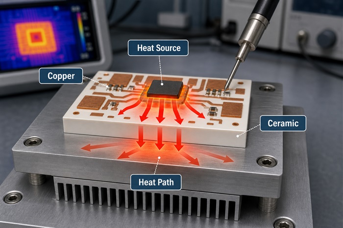
Designers should avoid placing heat-generating parts on small isolated pads without enough spreading copper or a defined path to the chassis or heat sink. For AlN and DBC/DCB substrates, the copper pattern may be part of the thermal structure, not only the electrical circuit. For alumina, the lower thermal conductivity can still work well when the heat load is moderate and the board outline, copper area, and mounting interface are designed together.
What Files Are Needed for a Ceramic PCB Prototype?
A ceramic pcb prototype RFQ should include more than Gerber files. The supplier also needs material, substrate thickness, copper thickness, surface finish, outline tolerance, hole and slot details, solder mask or protective coating needs, assembly method, operating environment, and target quantity.
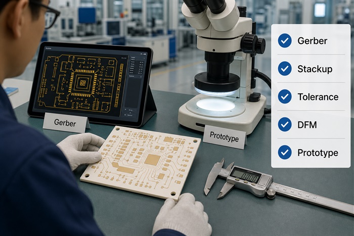
- Gerber files, drill files, and board outline drawing.
- Material requirement such as Al2O3, AlN, Si3N4, DBC, DPC, thick film, or thin film.
- Substrate thickness, copper thickness, surface finish, and metallization requirement.
- Critical tolerances for outline, hole, slot, pad, and flatness.
- Assembly information such as soldering, wire bonding, die attach, or connector load.
- Electrical requirements such as voltage, isolation distance, impedance, or current load.
- Thermal requirements such as heat source location, target heat path, and operating temperature.
For early-stage projects, a PCB prototype review is useful because it catches mismatches between the customer's preferred design and the selected ceramic process. It also helps separate must-have specifications from nice-to-have specifications that may increase cost or delay unnecessarily.
How Should Buyers Review a Ceramic PCB Design Before RFQ?
Buyers should review ceramic PCB designs by asking whether the material, process, geometry, thermal path, quality requirement, and quote package tell the same engineering story. If the Gerber says one thing, the BOM says another, and the drawing omits tolerances, the quotation will slow down or the prototype may need redesign.
| Review Item | Question to Ask | Why It Matters |
| Application | Is this for power, RF, LED, sensor, high voltage, or high temperature? | Application decides material and inspection priorities |
| Material | Is the substrate selected for heat, insulation, CTE, strength, or cost? | Wrong material can cause over-design or reliability risk |
| Process | Does the layout match DPC, DBC/DCB, thick film, or thin film? | Each process has different copper and feature limits |
| Mechanical design | Are slots, corners, edge clearance, and mounting holes reviewed? | Ceramic cracking often starts from stress concentration |
| Documentation | Are tolerances, surface finish, copper thickness, and special notes included? | Complete files reduce quotation back-and-forth |
BSTCeramicPCB can support ceramic board DFM communication for prototype and production projects. For faster review, send Gerber files, drawings, material targets, operating conditions, assembly needs, and expected quantity together instead of sending only a screenshot or incomplete layout export.
FAQ
What are ceramic PCB design guidelines?
They are the design rules and DFM checks used to make a ceramic circuit board manufacturable. They cover material choice, process route, copper features, vias, pads, board outline, thermal path, tolerances, and prototype documentation.
Can FR4 PCB design rules be used for ceramic PCB?
FR4 rules can help with general circuit planning, but they should not be copied directly. Ceramic substrates have different drilling, cutting, copper bonding, thermal, and mechanical stress limits, so the layout needs ceramic-specific DFM review.
Which ceramic material is best for PCB design?
There is no universal best material. Alumina is common and cost-effective, AlN fits higher thermal conductivity needs, Si3N4 supports tougher power cycling applications, and BeO requires special handling and supplier confirmation.
What is the difference between DPC and DBC ceramic PCB design?
DPC is often used for finer circuit features and thinner copper, while DBC/DCB is usually selected for thicker copper and power substrate applications. The right choice depends on current load, thermal path, feature size, and reliability requirements.
Can ceramic PCB boards have vias?
Some ceramic PCB processes can support vias, but the via type, diameter, filling, plating, and cost depend on material and process route. Always confirm via capability before finalizing a multilayer or double-sided ceramic design.
What copper thickness should a ceramic PCB use?
Copper thickness should be selected from current load, heat spreading, process route, spacing, and assembly method. Heavy copper may improve current and thermal performance, but it can require larger spacing and stronger DFM review.
What standards apply to ceramic circuit board design?
General PCB standards can guide documentation and quality expectations, but ceramic PCB design also depends on supplier-specific material and process capability. For critical applications, confirm standards, inspection criteria, and acceptance rules during RFQ.
What files are required for a ceramic PCB prototype?
Provide Gerber files, drill files, board outline drawing, material requirement, substrate thickness, copper thickness, surface finish, tolerances, assembly notes, operating conditions, and expected quantity. A complete package helps avoid quotation delays.
Why do ceramic PCB designs crack or fail?
Failures can come from sharp corners, poor slot design, high mounting stress, thermal cycling mismatch, insufficient edge clearance, improper copper geometry, or handling damage. DFM review should address mechanical stress as early as electrical layout.
How should ceramic PCB cost be controlled?
Cost is controlled by choosing the necessary material and process rather than the most advanced option by default. Avoid unnecessary fine features, oversized substrates, excessive tolerances, over-thick copper, and late design changes after prototype review.
When should I ask a supplier to review ceramic PCB design rules?
Ask before final layout release, especially when the design includes vias, slots, heavy copper, fine traces, high voltage, high heat, special surface finish, or tight mechanical tolerances. Early review is cheaper than redesign after quotation.
Can BSTCeramicPCB help review ceramic PCB design files?
Yes. BSTCeramicPCB can review ceramic PCB files for material choice, manufacturability, prototype preparation, and quotation guidance when customers provide complete design files and application requirements.
Conclusion
Ceramic PCB design guidelines should connect material choice, copper layout, vias, pads, thermal path, mechanical stress, process route, and prototype documentation. The best design is not the one with the most aggressive rules; it is the one that fits the application and can be manufactured repeatably.
If you are preparing a ceramic PCB board or ceramic pcb prototype, BSTCeramicPCB can help review your files, material options, DFM risks, and quotation details. Send your requirements to sales@bstceramicpcb.com or contact BSTCeramicPCB for engineering support.
 Products
 About us
 Contact us



