






















































 HOME
HOME

-

Ceramic PCB for Humanoid Robot joint actuators
2026 04,07 -
LTCC PCB Surprises: What Most People Miss
2025 12,09 -
Step-by-Step Guide to DPC PCB Design for Sensor Systems
2025 12,03 -
Ceramic PCBs Essential Benefits and Applications
2025 12,01 -
How Al2O3 DPC Ceramic Substrate PCB Enhances Heat Dissipation in Modern Electronics?
2025 11,28 -
How to Choose Between Ceramic, FR4, and Metal Core PCBs
2025 11,27 -
DPC Ceramic PCB Materials: Surprising Science Inside
2025 11,26 -
Wire bondable 2-layer Alumina substrates PCB | Bstceramic PCB
2025 09,22 -
Silicon Nitride Substrate, Silicon Nitride Ceramic Substrate Formula
2025 05,08 -
What is thick film ceramic PCB?
2023 08,02
Ceramic PCB Operate Temperature Range: Limits for Materials and Assemblies
Ceramic PCB operate temperature range is not one universal number. For many component-populated ceramic PCB assemblies, -55°C to +125°C or +150°C is a practical starting qualification window, while a specially engineered bare or metallized ceramic circuit can work at much higher temperatures. The final limit is set by the weakest material or interface in the complete assembly, not by the ceramic alone.
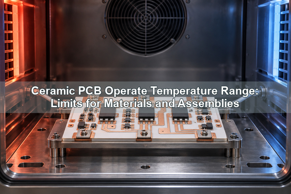
This distinction matters when a drawing simply says “high-temperature ceramic PCB.” Alumina, aluminum nitride and silicon nitride remain stable far beyond normal electronic component ratings, but copper attachment, thick-film paste, surface finish, solder, die attach, wire bonds, connectors and encapsulants may not. A useful specification therefore defines continuous operating temperature, short peak temperature, cycle profile, atmosphere and required life.
What Does Ceramic PCB Operating Temperature Range Mean?
The operating range is the minimum and maximum temperature at which the finished circuit must meet its electrical, mechanical and dimensional requirements. It is different from the ceramic firing temperature, the copper-bonding temperature and the maximum no-load temperature of a bare ceramic coupon.
Three temperature terms should be separated in a drawing or manufacturing inquiry:
- Continuous operating temperature: the temperature the circuit must withstand for most of its service life.
- Short-term peak temperature: a temporary excursion during startup, reflow, sterilization or an abnormal load, with a defined duration.
- Storage temperature: the non-operating limit for shipping or storage; it does not prove powered reliability.
The specification should also state whether the quoted value refers to ambient air, ceramic surface, baseplate, copper pad or semiconductor junction temperature. These locations can differ significantly under load.
What Is a Realistic PCB Temperature Range?
For an assembled ceramic PCB, -55°C to +125°C is a common electronics qualification envelope, and +150°C is often evaluated for automotive, power and downhole designs. These values are starting points, not automatic ratings. A board using high-temperature die attach and bare-die interconnects may exceed them, while an assembly with a low-temperature connector, polymer coating or solder alloy may need a lower limit.
| Construction Level | Useful Planning Range | What Usually Sets the Limit |
|---|---|---|
| Component-populated ceramic PCB | Often -55°C to +125°C or +150°C | Components, joints, connectors and encapsulation |
| Bare metallized ceramic circuit | Application-specific; may be several hundred °C | Metal system, adhesion, oxidation and atmosphere |
| Unmetallized ceramic substrate | Much higher than normal electronics ranges | Ceramic grade, load, atmosphere and thermal shock |
Do not copy a bare-ceramic maximum into a PCBA specification. The valid pcb temp rating is the temperature at which the complete construction has been qualified for the required time and cycling profile.
How Does the Ceramic Material Affect Temperature Capability?
Material choice changes heat spreading, coefficient of thermal expansion (CTE), mechanical strength and thermal-shock behavior. It does not by itself establish the finished pcb operating temperature range.
| Ceramic Material | Main Temperature-Relevant Strength | Main Design Boundary | Practical Selection Logic |
|---|---|---|---|
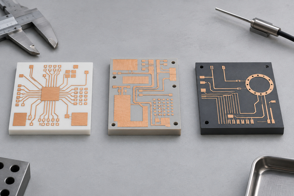
| Alumina (Al2O3) | Stable electrical insulation, mature processing and moderate thermal conductivity | Higher CTE and lower heat spreading than AlN; brittle under mechanical stress | Use when cost, insulation and proven processing matter more than maximum heat flux |
| Aluminum nitride (AlN) | High thermal conductivity with electrical insulation and a CTE closer to silicon | Moisture-sensitive powder history, brittle machining and higher cost | Use when junction temperature or local heat flux makes alumina inadequate |
| Silicon nitride (Si3N4) | High fracture toughness and strong thermal-cycle resistance | Higher material and process cost; process availability must be confirmed | Use for power modules with severe vibration, cycling or thick-copper stress |
An alumina DPC ceramic substrate for LED circuits is a relevant baseline when moderate thermal load and fine copper features are required. A double-sided aluminum nitride DPC circuit is better aligned with higher heat flux or a shorter thermal path.
Why Is the Bare Ceramic Limit Higher Than the Finished Circuit Limit?
A high-purity alumina body may tolerate a no-load temperature above 1,000°C, but that figure does not describe a copper-clad circuit carrying current. Heating changes copper strength, promotes oxidation, accelerates intermetallic growth and stresses the metal-to-ceramic interface. An assembled board adds more temperature-sensitive elements.
The finished limit should be calculated as a constraint chain:
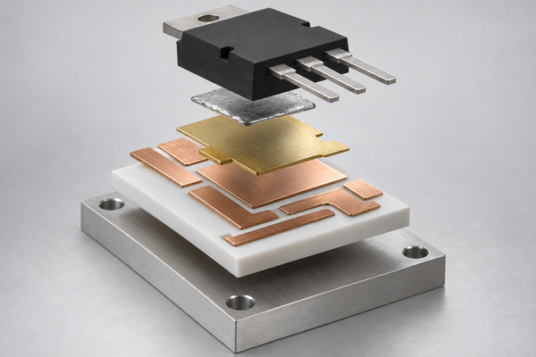
ceramic substrate → metallization interface → copper pattern → surface finish → joint material → component/package → coating or enclosure
The lowest qualified limit in that chain controls the assembly. This is why search results quoting 800°C for “ceramic PCB” can be misleading unless they define the construction, atmosphere, electrical load and service duration.
How Do Metallization and Assembly Materials Limit Temperature?
Thick film, thin film, DPC, DBC and AMB create different metal-to-ceramic interfaces. Their suitability depends on conductor thickness, current, temperature, atmosphere and cycling severity.
- Thick film: conductor and resistor pastes are fired onto ceramic. The circuit rating depends on the selected paste system, termination, overglaze and attached components, not the firing temperature.
- DPC and thin film: deposited or plated metal supports fine features, but diffusion barriers, plated finishes and adhesion must be checked at the intended temperature.
- DBC: thick copper provides current capacity and heat spreading, but copper expansion can load the ceramic during repeated hot-cold cycles.
- AMB: the active braze creates a robust copper-to-ceramic interface and is often selected with Si3N4 for high-reliability power cycling.
Our AMB ceramic PCB for IGBT power modules illustrates a construction chosen when thick copper and cyclic mechanical reliability matter. The exact temperature rating still requires confirmation of the braze, finish, die attach and module assembly.
Continuous Operation vs Short-Term Peak Temperature
A circuit that survives a five-minute peak at 200°C is not automatically suitable for 20,000 hours at 200°C. Time at temperature drives oxidation, diffusion, grain growth, polymer aging and joint fatigue. The peak specification therefore needs both temperature and duration.
Use a duty profile instead of one maximum value. For example: continuous 135°C at the ceramic surface, a 175°C peak for 10 minutes during startup, 1,000 cycles between -40°C and +150°C, and operation in dry nitrogen. This profile gives the manufacturer and test laboratory enough information to select materials and validate the design.
How Do Thermal Cycling and CTE Affect Reliability?
Repeated temperature change is often more damaging than a steady high temperature. Copper expands more than alumina, AlN or Si3N4. Each cycle therefore applies shear and peel stress at copper edges, large pads, vias, brazed interfaces and die-attach layers.
Reliability depends on temperature span, ramp rate, dwell time and cycle count. A slow cycle from 25°C to 125°C is not equivalent to a rapid -55°C to +150°C transition. Thick copper, large uninterrupted copper areas and abrupt corners can increase local stress. Balanced copper, rounded features, suitable ceramic thickness and controlled edge clearance can reduce risk, but final geometry should be reviewed for the selected metallization process.
What Ceramic PCB Design Rules Matter at High Temperature?
High-temperature ceramic pcb design rules should control both electrical performance and stress concentration. The most useful drawing inputs are finished values, because artwork dimensions alone do not define the manufactured circuit.
- Specify ceramic material, grade, thickness, outline and permitted edge chipping.
- Define finished copper thickness, minimum line/space and copper-to-edge clearance.
- Identify plated, filled, vented and mechanical holes separately.
- State surface finish and the next process: soldering, brazing, die attach or wire bonding.
- Avoid sharp internal copper corners and isolated heavy-copper islands where cycling stress can concentrate.
- Define flatness or bow under the correct measurement condition when large-area die attach is used.
- Keep temperature-sensitive connectors, adhesives and coatings away from local hot spots.
Thermal simulation should include interface resistance, baseplate and cooling conditions. High substrate conductivity helps only when heat can leave the substrate efficiently.
What Tests Confirm the Operating Temperature of a PCB?
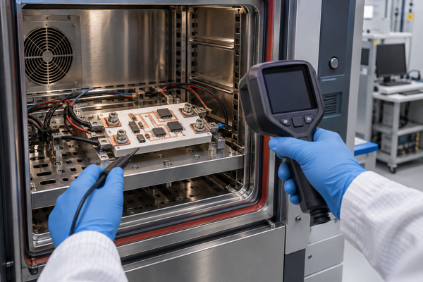
Qualification should reproduce the real failure mechanisms rather than only exposing an unpowered board to heat. A useful plan may combine:
- thermal cycling or thermal shock with specified endpoints, ramps, dwells and cycle count;
- high-temperature operating life under representative electrical load;
- insulation resistance and dielectric testing at temperature;
- metallization adhesion or peel testing before and after aging;
- cross-sectioning or acoustic inspection for interface cracks and voids;
- dimensional, flatness and electrical checks after exposure.
Coupons should contain the most demanding features: thick-copper edges, the smallest spacing, critical vias and representative large pads. Pass/fail criteria must be set before testing.
Which Applications Need a High-Temperature Ceramic PCB?
High-temperature ceramic circuits are useful when electrical insulation, heat spreading and dimensional stability must coexist. Typical applications include power modules near hot semiconductor junctions, LED and laser submounts, automotive under-hood electronics, industrial heaters and sensors, aerospace controls, downhole instrumentation and high-temperature measurement systems.
The application does not automatically justify the highest-cost ceramic. Alumina may be sufficient for a sensor with low heat flux, while AlN may reduce junction temperature in a compact laser or power converter. Si3N4 becomes attractive when mechanical shock and severe power cycling dominate. Selection should follow measured losses, allowable junction temperature, cooling path and reliability profile.
What Should You Provide for a Temperature-Rated Ceramic PCB Quote?
A useful quote package should allow the manufacturer to price the actual risk, not guess a generic pcb temperature range. Include:
- minimum and maximum continuous operating temperatures;
- peak temperature, duration and number of events;
- storage range and thermal-cycle profile;
- atmosphere, pressure, humidity and chemical exposure;
- ceramic material or performance target;
- circuit drawing, finished copper thickness and surface finish;
- assembly scope, component list and joining process;
- maximum voltage, current, power loss and hot-spot map;
- test method, sample quantity and acceptance criteria;
- prototype and production quantities.
At BSTCeramicPCB, we use these inputs to review the substrate, metallization and assembly boundaries together. If a requirement is still provisional, identify it as a target so prototype testing can establish a defensible production specification.
FAQ
Can a ceramic PCB operate at 800°C?
A bare ceramic or specialized metallized structure may tolerate very high temperature, but 800°C should not be treated as a universal ceramic PCB rating. Copper oxidation, metallization, joints, finishes, components and atmosphere must all be designed and qualified for that condition.
Is alumina or AlN better for high temperature?
AlN spreads heat much more effectively, while alumina is usually more economical and broadly available. Maximum service temperature alone rarely decides between them; heat flux, CTE, moisture control, mechanical loading and process cost are more useful criteria.
Does ceramic PCB temperature rating equal Tg?
No. Tg describes the glass transition of polymer-based laminates such as FR-4. Dense ceramic substrates do not use Tg as their primary temperature limit. The relevant limits come from ceramic properties and the complete metal, joint and component system.
What is the difference between operating and storage temperature?
Operating temperature applies while the circuit is powered and must meet performance requirements. Storage temperature applies when it is not operating. A wide storage range does not prove that the circuit can carry current or dissipate heat across the same range.
How is a high-temperature ceramic PCB qualified?
Qualification normally combines temperature exposure with electrical load, cycling, adhesion, insulation and structural inspection. The test profile should match the real operating range, ramp rate, dwell, atmosphere and expected lifetime.
The correct ceramic PCB operate temperature range is a system rating, not a single ceramic-material property. Send your temperature profile, circuit drawing, material target and test requirements to sales@bstceramicpcb.com for a manufacturability and quotation review.
 Products
 About us
 Contact us



