






















































 HOME
HOME

-

Ceramic PCB for Humanoid Robot joint actuators
2026 04,07 -
LTCC PCB Surprises: What Most People Miss
2025 12,09 -
Step-by-Step Guide to DPC PCB Design for Sensor Systems
2025 12,03 -
Ceramic PCBs Essential Benefits and Applications
2025 12,01 -
How Al2O3 DPC Ceramic Substrate PCB Enhances Heat Dissipation in Modern Electronics?
2025 11,28 -
How to Choose Between Ceramic, FR4, and Metal Core PCBs
2025 11,27 -
DPC Ceramic PCB Materials: Surprising Science Inside
2025 11,26 -
Wire bondable 2-layer Alumina substrates PCB | Bstceramic PCB
2025 09,22 -
Silicon Nitride Substrate, Silicon Nitride Ceramic Substrate Formula
2025 05,08 -
What is thick film ceramic PCB?
2023 08,02
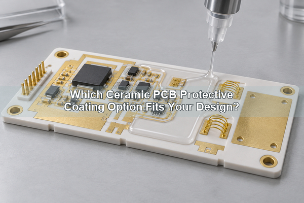
Which Ceramic PCB Protective Coating Option Fits Your Design?
A ceramic PCB protective coating option should protect the vulnerable parts of a ceramic circuit without blocking heat flow, electrical contact, wire bonding, soldering or later rework. The ceramic substrate itself is stable and non-hygroscopic compared with many organic laminates, but its conductors, solder joints, components and interfaces can still fail from condensation, chemicals, particles, corrosion or mechanical damage.
What Does a Ceramic PCB Protective Coating Need to Protect?
Start with the failure path, not the coating name. An assembled ceramic PCB can expose printed conductors, plated copper, wire bonds, component terminations, solder joints and high-voltage spacing. A coating may need to prevent moisture-assisted leakage, corrosion, conductive contamination, chemical attack or abrasion. It may also need to stabilize a printed resistor or dielectric area.
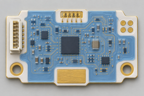
The coating boundary matters as much as the material. Connector contacts, wire-bond pads, test points, grounding pads, solderable terminals and thermal interfaces normally need defined keep-out areas. Applying one continuous layer over every surface can create an assembly or heat-transfer problem while solving an environmental one.
Which Ceramic PCB Protective Coating Options Are Available?
The main choices differ in how they are applied, when they are added and whether they remain reworkable.
| Protection option | Typical role | Main advantage | Main limitation |
|---|---|---|---|
| Fired glass overglaze | Covers selected thick-film conductors, resistors or dielectric features before assembly | Inorganic layer compatible with a qualified print-and-fire stack | Requires compatible paste and firing sequence; not a field-applied assembly coating |
| Acrylic conformal coating | General moisture and contamination protection | Fast cure and relatively easy rework | Limited chemical and high-temperature performance compared with harder systems |
| Silicone conformal coating | Wide-temperature and moisture protection | Remains flexible and tolerates thermal movement | Can be harder to clean or recoat; silicone contamination control matters |
| Urethane conformal coating | Chemical, moisture and abrasion resistance | Tougher barrier than many acrylics | Removal and rework can be difficult |
| Epoxy coating | Hard, durable protection | Strong chemical and mechanical resistance | Low reworkability and higher stress risk if the stack is poorly matched |
| Parylene | Thin, uniform vapor-deposited barrier | Excellent coverage of complex geometry and small gaps | Specialized process, masking effort and difficult rework |
| Potting or encapsulation | Full-volume environmental and mechanical protection | Strong isolation and mechanical support | Adds mass, traps heat, increases stress and usually prevents repair |
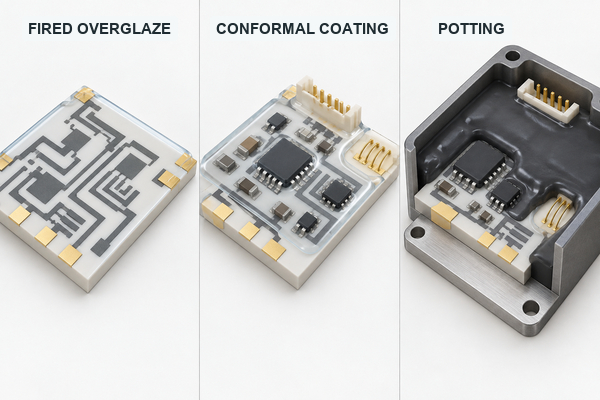
How Is Fired Glass Overglaze Different from Conformal Coating?
Fired glass overglaze is part of the thick-film ceramic process. It is printed over selected features and fired as a compatible inorganic layer. It can protect conductor edges, printed resistors or dielectric areas while leaving assembly pads open. Its chemistry and firing profile must match the underlying ceramic and thick-film materials.
Conformal coating is normally applied after component assembly. It follows the finished three-dimensional surface and protects components, joints and exposed circuitry. It is commonly a polymer, although parylene uses a vapor-deposition route. The two methods can coexist when an overglazed ceramic circuit is later assembled and selectively conformal coated.
Our automotive oil-level sensor ceramic circuit uses a 96% alumina substrate, AgPd conductors and green glass glaze. This is an example of a fired protective layer defined as part of the ceramic circuit stack, not a substitute for every post-assembly environmental coating.
When Should You Use Acrylic, Silicone, Urethane, Epoxy, or Parylene?
Choose the polymer from the operating environment, temperature range, rework plan and application process. A chemistry with excellent moisture resistance can still be unsuitable if it softens at the operating temperature, attacks a component material, cannot cure under a package or blocks later bonding.
| Design condition | Usually worth evaluating first | Selection check |
|---|---|---|
| Moderate humidity with expected repair | Acrylic | Confirm solvent compatibility, cure and required thickness |
| Wide temperature range or repeated thermal cycling | Silicone | Check modulus, adhesion, outgassing and contamination controls |
| Oils, fuels, solvents or abrasion | Urethane | Confirm chemical exposure, cure completeness and removal method |
| Hard, permanent protection | Epoxy | Model stress and heat flow; accept limited rework |
| Complex topography or very uniform thin coverage | Parylene | Define masking, adhesion promotion and specialized process controls |
Aerosol spray can be useful for low-volume work, but a spray product name does not define final coverage. Edge buildup, shadowing under components, overspray and inconsistent thickness must still be controlled.
When Is Potting or Encapsulation the Better Choice?
Potting is appropriate when the assembly needs strong mechanical support, high environmental isolation or tamper resistance and repair is not expected. It can protect against vibration, salt, liquids and debris more completely than a thin conformal layer.
It is unnecessary when a selective coating meets the exposure requirement. Potting increases weight and material volume, can trap heat around components and creates thermal-expansion stress between the compound, ceramic, metal and packages. Define the potting depth, cure exotherm, modulus, adhesion surfaces and thermal path before selecting it.
Do Ceramic PCBs Need Coating If the Substrate Is Already Inorganic?
Not always. A bare ceramic substrate does not need coating simply because it is ceramic. The decision depends on the exposed circuit and the operating environment. A sealed module with protected conductors may need no additional coating, while an open sensor board in condensation or corrosive vapor may require selective protection.
The substrate material also does not prevent corrosion of silver-bearing pastes, copper features, component leads or solder joints. High electric-field regions can collect ionic contamination even when the ceramic itself remains dimensionally stable. The protection plan should therefore identify the exposed metallization and assembly interfaces rather than treating the substrate as the only risk.
For a thick-film alumina circuit with integrated resistors, the drawing should distinguish resistor, conductor, dielectric, overglaze and assembly-pad areas. That separation determines what can be covered during ceramic processing and what must remain accessible during assembly and test.
How Do Temperature, Voltage, Moisture, and Chemicals Change the Selection?
Environmental requirements should be translated into measurable limits.
| Stress | What to specify | Why it changes the coating choice |
|---|---|---|
| Temperature | Continuous range, peak, dwell time and thermal-cycle profile | Changes cure margin, modulus, adhesion and cracking risk |
| Voltage | Working voltage, transient level, spacing and contamination condition | Determines whether coating thickness and coverage support insulation needs |
| Moisture | Condensation, immersion, humidity level and duration | Separates splash protection from long-term moisture-barrier needs |
| Chemicals | Exact fluid, concentration, temperature and contact time | Generic “chemical resistant” claims do not predict compatibility |
| Mechanical load | Vibration, shock, abrasion and handling | May favor a tougher coating, staking or encapsulation |
| Cleanliness | Ionic residue limit and cleaning process | Contamination trapped under a coating can accelerate leakage and corrosion |
For high-temperature assemblies, material selection must cover both the substrate process and the post-assembly coating. Our HTCC ceramic PCB for signal-converter applications is specified for a published operating range of -40 to 300 degrees C. A polymer coating cannot be assumed to share that range; its own qualification and the assembled stack still need review.
How Do Protective Coatings Affect Thermal Performance?
Ceramic PCBs are often selected to move heat, so the coating must not interrupt the intended path. A thin layer over low-power traces may have little system impact, but coating a component base, heat-spreader contact, metallized mounting pad or clamping surface adds a thermal interface and can reduce contact quality.
Thermal analysis should use the actual coating thickness, conductivity and covered area. Potting compounds need particular attention because a large volume can either assist heat spreading or insulate hot components depending on formulation and geometry. Keep direct ceramic-to-heatsink and metal-to-heatsink surfaces uncoated unless the thermal design explicitly includes the coating.
What Areas Must Be Masked Before Coating?
The fabrication package should identify every keep-out area instead of relying on production judgment. Common exclusions include:
- gold or aluminum wire-bond pads;
- connector contacts and press-fit areas;
- test points and programming pads;
- solder pads needed after coating;
- grounding and chassis-contact surfaces;
- mounting holes, threads and datum features;
- optical windows, sensors and adjustable components;
- heat-spreader and heatsink contact surfaces.
Masking must survive the application and cure process without leaving residue. Its removal method must not lift fragile wire bonds, damage printed features or chip the ceramic edge.
Which Coating Defects Cause Reliability Problems?
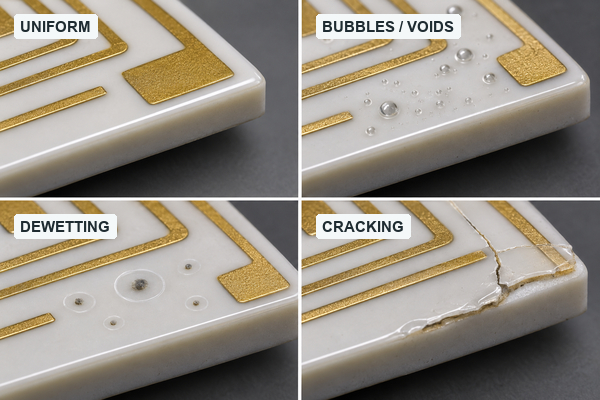
The defect pattern often identifies the process problem.
| Defect | Common contributor | Practical response |
|---|---|---|
| Dewetting or fisheyes | Oil, flux, silicone or low-surface-energy contamination | Improve cleaning and verify surface condition before coating |
| Bubbles or voids | Trapped air, aggressive application, solvent or cure profile | Control dispensing, dwell, viscosity and cure |
| Shadowed or thin areas | Dense components, wrong spray angle or poor flow | Adjust application path or use a process with better coverage |
| Cracking | Excess thickness, rigid coating, thermal mismatch or sharp geometry | Reduce buildup and review modulus and thermal cycling |
| Delamination | Contamination, moisture, poor adhesion or incompatible materials | Qualify cleaning, adhesion promotion and material compatibility |
| Coating on keep-outs | Weak masking definition or removal control | Add drawing-controlled boundaries and post-coat inspection |
How Should Adhesion, Coverage, and Cure Be Verified?
Inspection should match the risk. Visual inspection can confirm coverage, masking boundaries, bubbles, bridging and damage. Fluorescent tracer inspection can help reveal missed areas when the selected coating supports it. Thickness measurement is useful where electrical insulation or mechanical buildup depends on a controlled layer.
Adhesion and cure should be verified on the actual surface finish and cleaning process. Qualification may include cross-hatch or pull testing where appropriate, insulation resistance, dielectric tests, humidity exposure, thermal cycling and chemical resistance. A coating that passes on bare alumina may behave differently over gold, AgPd, copper, solder mask, flux residue or a molded package.
What Design and Manufacturing Data Should You Provide?
Provide the following information before material selection and quotation:
- ceramic type, thickness, metallization and surface finish;
- assembled or bare-board coating stage;
- coating coverage drawing and explicit keep-out dimensions;
- operating and storage temperatures, voltage and spacing requirements;
- humidity, condensation, immersion and chemical exposures;
- target coating type or required performance if the chemistry is open;
- nominal thickness, cure restrictions and allowable process temperature;
- rework, soldering, wire-bonding and thermal-interface requirements;
- required inspection, qualification and acceptance records;
- prototype quantity, production forecast and packaging constraints.
If the design is still open, mark the non-negotiable performance requirements and let the coating chemistry remain a reviewed output. Naming a material too early can lock the project into poor reworkability, unnecessary cost or an incompatible cure.
FAQ
What are the different types of PCB protective coatings?
Common options include acrylic, silicone, urethane, epoxy and parylene conformal coatings, plus potting compounds. Thick-film ceramic circuits may also use fired glass overglaze as part of the printed and fired layer system.
Which protective chemical coating is applied on a PCB?
There is no universal chemical. The correct choice depends on temperature, moisture, chemicals, voltage, rework and application method. Acrylic is often considered for reworkable general protection; silicone for wide temperature ranges; urethane or epoxy for tougher chemical and mechanical protection; and parylene for thin, uniform coverage.
Is glass glaze the same as conformal coating?
No. Glass glaze is normally an inorganic fired layer used in a compatible thick-film ceramic process. Conformal coating is usually applied after assembly and follows the finished components and solder joints.
Can conformal coating cover wire-bond pads?
Not before wire bonding. Bond pads need clean, controlled metal surfaces. If coating is added after bonding, the material and process must be qualified for the wires, bond heels, package and required electrical performance.
Can protective coating reduce ceramic PCB heat dissipation?
Yes, if it covers a thermal contact or creates a thick insulating layer around hot components. The effect depends on thickness, conductivity, coverage and the complete heat path.
Final Selection Checklist
The right ceramic PCB protective coating option protects the actual failure-sensitive features while preserving assembly access and heat flow. Before release, confirm the exposure, coating stage, material compatibility, coverage map, keep-outs, cure, inspection method, rework plan and thermal path.
BSTCeramicPCB can review the ceramic stack, metallization, assembly interfaces and protection requirements before quotation. Send the drawing, environment, test requirements and expected quantity to sales@bstceramicpcb.com.
 Products
 About us
 Contact us



