






















































 HOME
HOME


-

Ceramic PCB for Humanoid Robot joint actuators
2026 04,07 -
LTCC PCB Surprises: What Most People Miss
2025 12,09 -
Step-by-Step Guide to DPC PCB Design for Sensor Systems
2025 12,03 -
Ceramic PCBs Essential Benefits and Applications
2025 12,01 -
How Al2O3 DPC Ceramic Substrate PCB Enhances Heat Dissipation in Modern Electronics?
2025 11,28 -
How to Choose Between Ceramic, FR4, and Metal Core PCBs
2025 11,27 -
DPC Ceramic PCB Materials: Surprising Science Inside
2025 11,26 -
Wire bondable 2-layer Alumina substrates PCB | Bstceramic PCB
2025 09,22 -
Silicon Nitride Substrate, Silicon Nitride Ceramic Substrate Formula
2025 05,08 -
What is thick film ceramic PCB?
2023 08,02
Ceramic PCB Thermal Cycling Failure: Causes, Materials and Test Checks
Published:
Ceramic PCB thermal cycling failure occurs when repeated heating and cooling create stress between the ceramic substrate, copper metallization, solder joints, components and mounting structure. The main design controls are ceramic material, CTE match, copper thickness, ceramic PCB thickness, thermal gradient, bonding process and the thermal cycle test profile.
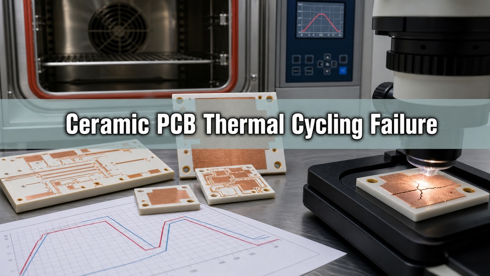
A ceramic PCB may have excellent thermal conductivity and electrical insulation, but those properties do not automatically prevent fatigue. Thermal cycling reliability depends on how the complete stack expands, contracts, transfers heat and constrains mechanical movement over hundreds or thousands of cycles.
What Causes Ceramic PCB Thermal Cycling Failure?
Thermal cycling failure is caused by repeated thermo-mechanical strain. Ceramic, copper, solder, die attach materials and mounted components expand at different rates as temperature changes. When these layers are bonded together, the mismatch creates shear and tensile stress at interfaces, copper edges, vias, solder joints and ceramic corners.
The highest-risk areas are usually copper-to-ceramic interfaces, large copper islands, sharp internal corners, plated vias, soldered component joints and mounting holes. Designs with heavy copper, rapid temperature transitions, thick ceramic sections or uneven heat sources need earlier reliability review because local stress can be much higher than the average board temperature suggests.
How Does CTE Mismatch Damage Ceramic PCBs?
CTE mismatch damages ceramic PCBs by forcing bonded materials to move by different amounts during each heating and cooling cycle. Copper has a much higher coefficient of thermal expansion than common ceramic substrates, so copper areas tend to expand and contract more than the ceramic base. The bonded interface carries the resulting strain.
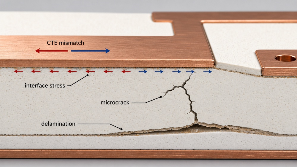
In practical ceramic circuit design, CTE is not reviewed as a single material value. The stack should be evaluated as a structure: copper thickness, copper area, ceramic thickness, metallization process, solder material, component size and fixture design all change the strain path. This is why a ceramic PCB with good material data can still fail when copper distribution or mounting is not controlled.
How Does Ceramic PCB Thermal Conductivity Affect Thermal Cycling?
Ceramic PCB thermal conductivity affects how quickly heat spreads away from the heat source and how steep the temperature gradient becomes across the board. A high-conductivity substrate can reduce hot spots, but it does not eliminate thermal fatigue if the design still has a large CTE mismatch, thick copper imbalance or constrained mounting.
Al2O3 is often used for cost-effective ceramic PCBs, but its thermal conductivity is lower than AlN. AlN provides stronger heat spreading, while Si3N4 is often considered when fracture toughness and cycling reliability are more important than maximum conductivity. For power substrates, the material decision should balance heat flow and mechanical reliability rather than treating thermal conductivity as the only ranking factor.
How Do Al2O3, AlN and Si3N4 Compare Under Thermal Cycling?
Al2O3, AlN and Si3N4 behave differently under thermal cycling because their thermal conductivity, CTE, toughness and process compatibility are different. The correct material depends on the failure mode that must be controlled: heat accumulation, ceramic cracking, copper interface fatigue or cost-sensitive production.
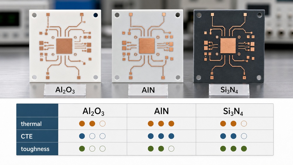
| Material | Thermal Cycling Strength | Typical Limitation | Engineering Use |
| Al2O3 | Mature, economical and suitable for many ceramic PCB applications | Lower thermal conductivity and lower fracture toughness than advanced ceramics | Cost-sensitive DPC, thick film and moderate-power ceramic circuits. |
| AlN | High thermal conductivity helps reduce hot spots | More brittle than Si3N4 in severe cycling conditions | High heat flux circuits, LED modules, laser drivers and compact power electronics. |
| Si3N4 | Strong fracture toughness and better cycling margin in demanding power modules | Higher material and process cost | AMB substrates, automotive power modules and high-reliability cycling applications. |
BSTCeramicPCB can review material selection for Alumina DPC ceramic substrate PCB, AlN ceramic circuits and DBC/DCB structures when the operating profile includes repeated thermal cycling.
How Does Ceramic PCB Thickness Influence Thermal Stress?
Ceramic PCB thickness influences both heat flow and mechanical stiffness. A thinner ceramic layer can reduce thermal resistance, but it may also reduce mechanical margin under handling, mounting or localized copper stress. A thicker ceramic layer can improve rigidity and dielectric spacing, but it may increase the temperature drop through the substrate and change how stress concentrates around copper edges.
Thickness should be specified together with copper thickness, dielectric test requirement, outline size, hole position, soldering process and mounting method. A design that works at 0.38 mm ceramic thickness may not behave the same at 0.63 mm or 1.0 mm if copper coverage and heat source geometry remain unchanged.
Which Design Features Increase Thermal Cycling Failure Risk?
Thermal cycling risk increases when the ceramic PCB layout creates concentrated stress or uneven heating. The most common design features to review are large unbalanced copper areas, sharp copper corners, narrow ceramic webs, dense via fields near hot spots, holes close to board edges and stiff mounting points near the active heat source.
- Use rounded copper corners where process rules allow, especially around large copper islands.
- Avoid abrupt copper area changes that concentrate interface stress.
- Keep mounting holes and slots away from fragile ceramic sections when possible.
- Review copper symmetry on double-sided structures to reduce warpage.
- Define minimum ceramic web width around holes, slots and edge features.
- Check whether solder joints or wire bonds will experience repeated out-of-plane movement.
How Do DPC, DBC and AMB Processes Affect Reliability?
DPC, DBC and AMB processes create different copper-to-ceramic structures, so their thermal cycling behavior is not identical. DPC is useful for finer circuits and plated features, DBC/DCB is common for copper-on-ceramic power substrates, and AMB is often selected for high-reliability power modules using Si3N4 or AlN.
| Process | Thermal Cycling Consideration | Inspection Focus |
| DPC | Fine features and plated vias need adhesion and plating reliability control | Copper thickness, via plating, trace adhesion, surface finish and thermal shock evidence. |
| DBC/DCB | Heavy copper and large copper areas can create interface and ceramic stress | Bond quality, voids, ceramic cracks, warpage, copper etching and isolation test. |
| AMB | High-reliability substrates depend on braze quality and ceramic toughness | Braze layer, peel strength, voids, warpage, thermal cycling and power cycling evidence. |
For heavy copper or power module structures, DCB ceramic substrate PCB for power semiconductor options should be reviewed with copper thickness, ceramic material and test profile together.
What Failure Modes Should Be Checked After Cycling?
Thermal cycling inspection should look for both visible damage and hidden interface degradation. A ceramic PCB can pass a simple visual check but still have bond weakening, microcracks, increased resistance or insulation margin loss.
- Microcracks in ceramic near copper edges, holes, slots or corners.
- Delamination between copper, metallization layer and ceramic substrate.
- Warpage or bow that changes assembly contact or solder joint loading.
- Trace resistance drift caused by conductor cracking or interface damage.
- Insulation resistance drop after cycling, especially under humidity or high voltage.
- Solder joint fatigue around large components or stiff terminals.
- Void growth or bond degradation in DBC, AMB or soldered assemblies.
How Is a PCB Thermal Cycle Test Defined?
A PCB thermal cycle test is defined by the low temperature, high temperature, dwell time, ramp rate, transfer time, number of cycles, sample condition and pass/fail criteria. Without those details, the phrase "thermal cycle test" is too vague for supplier comparison or reliability planning.
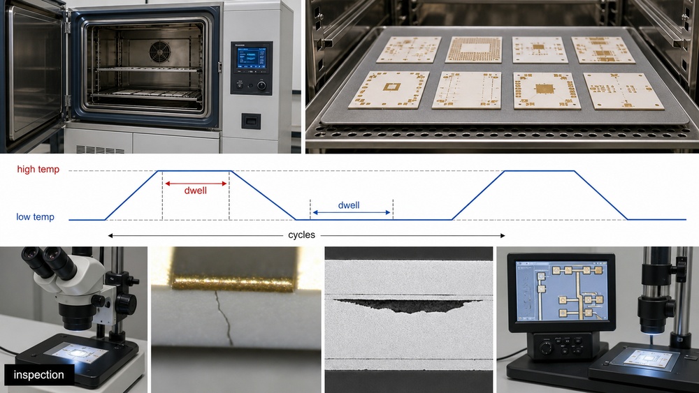
Common test planning details include the actual operating temperature range, worst-case storage temperature, power-on or non-operating condition, soldered or bare substrate state, electrical monitoring, insulation test interval and final cross-section requirement. Thermal cycling should not be confused with thermal shock: thermal shock uses faster transitions and usually creates more abrupt stress.
What RFQ Information Is Needed for Thermal Cycling Review?
A thermal cycling review needs enough information to connect the operating environment to the ceramic PCB structure. The RFQ should include drawings, stack details, thermal requirements and reliability expectations rather than only a material name.
- Ceramic material: Al2O3, AlN, Si3N4 or open for engineering review.
- Ceramic thickness, copper thickness, copper coverage and minimum line/space.
- Operating temperature range, thermal cycling range and number of cycles.
- Heat source size, power density, mounting method and heat sink interface.
- Process route: thick film, thin film, DPC, DBC/DCB or AMB.
- Required inspections: visual, X-ray, cross-section, adhesion, isolation or resistance monitoring.
- Prototype quantity, annual volume and failure criteria for qualification.
For quotation or material review, send drawings and test requirements through the ceramic substrate PCB quote page or contact BSTCeramicPCB directly at sales@bstceramicpcb.com.
How Can Ceramic PCB Thermal Cycling Failure Be Reduced?
Ceramic PCB thermal cycling failure can be reduced by matching material properties, controlling copper geometry, choosing a suitable metallization process, defining realistic thickness limits and validating the design with an appropriate thermal cycle test.
Practical improvements include balanced copper design, rounded copper features, suitable ceramic thickness, controlled solder joint geometry, compliant mounting where possible, and early prototype testing before production tooling or volume ordering. For severe cycling conditions, Si3N4 AMB or carefully designed AlN/DBC structures may be more appropriate than a standard alumina board.
FAQ About Ceramic PCB Thermal Cycling Failure?
1. Is thermal cycling the same as thermal shock?
No. Thermal cycling usually uses controlled transitions between high and low temperatures, while thermal shock uses faster temperature changes or transfer between zones. Thermal shock is generally more aggressive for ceramic cracking and interface stress.
2. Does higher ceramic PCB thermal conductivity prevent failure?
No. Higher thermal conductivity can reduce hot spots, but thermal cycling reliability also depends on CTE mismatch, copper thickness, ceramic thickness, solder joints, mounting and process quality.
3. Why does CTE matter in ceramic PCB design?
CTE determines how much each material expands and contracts with temperature. Mismatch between copper, ceramic, solder and components creates cyclic strain that can lead to cracking, delamination or fatigue.
4. Which ceramic material is best for thermal cycling?
There is no single best material. Al2O3 is practical and economical, AlN improves heat spreading, and Si3N4 often provides better fracture toughness for demanding power cycling and thermal cycling structures.
5. Should thermal cycling be tested on bare ceramic substrates or assembled boards?
Both may be useful. Bare substrate testing checks ceramic and metallization integrity, while assembled board testing captures solder joints, components, mounting stress and real electrical behavior.
Conclusion
Ceramic PCB thermal cycling failure is controlled by the complete structure, not by one material property. Thermal conductivity, CTE, ceramic PCB thickness, copper geometry, metallization process, mounting and test conditions all affect reliability. A useful design review should define the expected temperature range, number of cycles, inspection criteria and failure limits before production.
BSTCeramicPCB can review ceramic PCB drawings for material selection, DPC/DBC/AMB process suitability, copper design and thermal cycle test planning. For technical review or quotation, send your drawing package and reliability requirements to sales@bstceramicpcb.com.
 Products
 About us
 Contact us



