






















































 HOME


-

Ceramic PCB for Humanoid Robot joint actuators
2026 04,07 -
LTCC PCB Surprises: What Most People Miss
2025 12,09 -
Step-by-Step Guide to DPC PCB Design for Sensor Systems
2025 12,03 -
Ceramic PCBs Essential Benefits and Applications
2025 12,01 -
How Al2O3 DPC Ceramic Substrate PCB Enhances Heat Dissipation in Modern Electronics?
2025 11,28 -
How to Choose Between Ceramic, FR4, and Metal Core PCBs
2025 11,27 -
DPC Ceramic PCB Materials: Surprising Science Inside
2025 11,26 -
Wire bondable 2-layer Alumina substrates PCB | Bstceramic PCB
2025 09,22 -
Silicon Nitride Substrate, Silicon Nitride Ceramic Substrate Formula
2025 05,08 -
What is thick film ceramic PCB?
2023 08,02
Custom Ceramic PCB Manufacturer Serving Germany
Published:
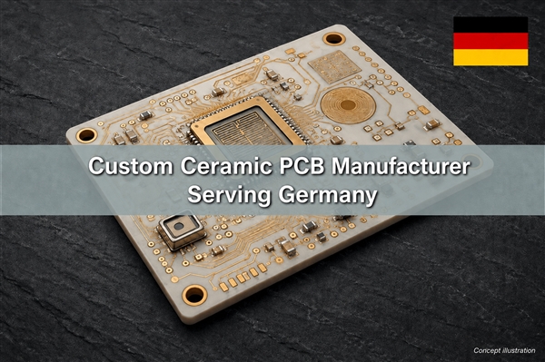
At BSTCeramicPCB, we are a custom ceramic PCB manufacturer serving Germany, manufacturing ceramic circuits in China for German engineering teams. Ceramic PCBs for Germany precision sensor designs must preserve the relationship between the sensing element, metal pattern and mechanical reference. Our thin-film, thick-film, DPC and other ceramic process options are supported by manufacturing review, prototypes and agreed assembly work, including coordination with FPC and rigid-flex parts used elsewhere in the sensor system.
Manufacture Around the Sensor Function
A precision sensor circuit needs manufacturing decisions tied to its measurement task. The required pad geometry, conductor resistance and mounting references may matter more than a headline material property. We review those relationships before choosing a ceramic process.
For German instrument and industrial-electronics teams, this can mean a compact ceramic sensing element linked to a conventional control board, rather than making the whole system ceramic. Semiconductor and medical instruments can use the same functional separation where a small critical circuit requires a controlled ceramic platform.
Thin-Film Features and Plated Copper Serve Different Needs
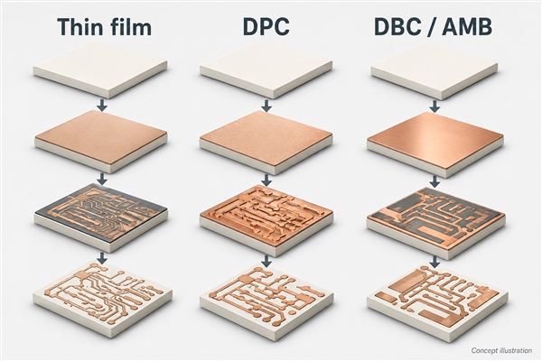
Our thin-film ceramic circuits for medical equipment offer a fine-pattern route, while DPC ceramic PCB for sensors use plated copper circuitry. Thin film can support smaller metal features; plated copper can be useful when the conductor cross-section is a larger part of the electrical requirement.
Our standard thin-film capability lists 20 um minimum line width with film thickness below 3 um. DPC capability lists 75/75 um minimum line width/spacing. These figures describe different process conditions and require engineering review; they are not interchangeable layout limits or a guarantee for every substrate and metal stack.
Control Geometry Relative to a Mechanical Datum
The useful dimension is often the position of a pad or sensing feature relative to a mounting reference, not only the overall board size. A sensor that is electrically correct may still perform inconsistently if assembly changes that relationship.
| Feature to control | Reason it matters |
|---|---|
| Pad-to-datum position | Maintains alignment with the sensing element or external interface. |
| Ceramic outline and edge condition | Supports repeatable mounting without concentrating stress at a defect. |
| Metallization definition | Controls the active conductor geometry and available attachment area. |
| Finished substrate flatness | Influences seating, attachment thickness and mechanical repeatability. |
Specify the datum scheme consistently across the circuit drawing and assembly drawing. Tightening every tolerance indiscriminately adds complexity; focus the control on features that influence the measurement.
Select Ceramic for Stability as Well as Heat Transfer
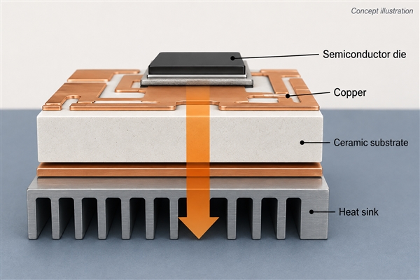
Alumina is a practical starting point for many electrically insulating sensor substrates. Aluminum nitride may be preferable where local heat needs to pass through a small area. The thermal conductivity alone does not establish sensor accuracy or long-term stability.
Check thermal gradients, expansion mismatch and the temperature sensitivity of the actual sensing circuit. A mechanically constrained substrate may transfer expansion stress into an attachment joint. A heat sink or housing interface can also dominate the temperature distribution, so verify the mounted assembly rather than relying only on a ceramic data sheet.
Use Thick-Film and Co-Fired Routes Where They Add Function
Our thick-film ceramic substrates for medical devices are relevant when printed functional layers belong in the design. Our LTCC ceramic substrates for sensors provide a co-fired multilayer route for suitable circuits. These options add manufacturing choices, but also introduce their own material and firing constraints.
Do not treat LTCC as simply a thinner version of a DPC board. Its stacked ceramic-tape and co-firing process requires coordinated conductor materials, internal features and dimensional planning. The best route is the one that supports the required function with a controllable process, not the route with the longest feature list.
Make Assembly Inspection Relevant to Sensor Performance
Inspection should cover the assembly features capable of changing the measurement. Pad contamination, attachment placement, excess solder and stress from mounting can matter even when the conductor pattern passes an electrical check.
We discuss fabrication and assembly inspection as separate but connected stages. Confirm which acceptance criteria apply to the bare circuit and which require an assembled prototype. Repeatability testing should use the intended mounting arrangement so that assembly variation is not hidden by a different laboratory fixture.
Connect Ceramic Sensors with FPC or Rigid-Flex
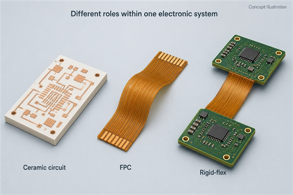
FPC can route a sensor connection through a confined housing, while rigid-flex can combine mounted components and flexible interconnect regions. Neither construction makes the ceramic sensing substrate flexible. Their role is to connect and position the electronics around it.
We can coordinate the ceramic and associated interconnect requirements for German projects. Include strain relief and adequate support at the ceramic connection, and keep the flex bend away from the attachment. If the connection moves repeatedly in service, the flex design requires a defined movement duty rather than an assumed static installation bend.
Separate Process Time from Delivery Planning
The production schedule follows the selected ceramic process, material availability and inspection scope. Thin-film deposition and patterning, thick-film printing and firing, and co-fired multilayer work have different stage requirements.
We confirm the build schedule after reviewing the actual design and quantity. Delivery to Germany should include a separate transport estimate, rather than adding an unsupported fixed shipping promise to a fabrication estimate. Where a prototype must pass measurement validation before volume release, include that decision point in the schedule.
Preserve Quality Evidence and Revision Control
For recurring sensor production, the approved material, metallization, finish and drawing revision must remain traceable. A change in the process or attachment system may require renewed comparison against the measurement baseline, even if a basic electrical test still passes.
We discuss current quality-system documentation and the relevant inspection records with the project team. Where ISO 9001 or medical-sector ISO 13485 documentation is required, its entity, scope and validity must match the claimed activity. Certification does not replace part-specific validation.
If you need a ceramic PCB manufacturer serving Germany, contact our team at sales@bstceramicpcb.com to discuss your ceramic circuit, prototype build, assembly scope and related FPC or rigid-flex requirements.
 Products
 About us
 Contact us



