






















































 HOME
HOME

-

Ceramic PCB for Humanoid Robot joint actuators
2026 04,07 -
LTCC PCB Surprises: What Most People Miss
2025 12,09 -
Step-by-Step Guide to DPC PCB Design for Sensor Systems
2025 12,03 -
Ceramic PCBs Essential Benefits and Applications
2025 12,01 -
How Al2O3 DPC Ceramic Substrate PCB Enhances Heat Dissipation in Modern Electronics?
2025 11,28 -
How to Choose Between Ceramic, FR4, and Metal Core PCBs
2025 11,27 -
DPC Ceramic PCB Materials: Surprising Science Inside
2025 11,26 -
Wire bondable 2-layer Alumina substrates PCB | Bstceramic PCB
2025 09,22 -
Silicon Nitride Substrate, Silicon Nitride Ceramic Substrate Formula
2025 05,08 -
What is thick film ceramic PCB?
2023 08,02
Custom Ceramic PCB Manufacturer Serving Israel
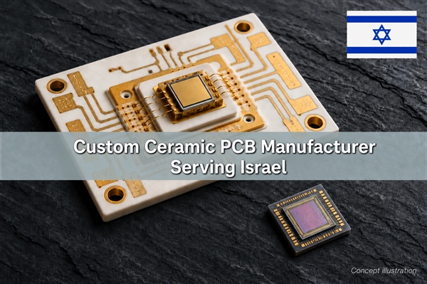
At BSTCeramicPCB, we are a custom ceramic PCB manufacturer serving Israel, manufacturing ceramic circuits in China for Israeli engineering teams. Ceramic PCBs for Israel laser and semiconductor modules need a controlled thermal path and a metal pattern suited to the attachment process. We support custom layouts, prototypes and assembly services for the ceramic circuit or agreed subassembly, while coordinating FPC and rigid-flex requirements where a compact module connects to its controller or instrumentation electronics.
Custom Ceramic Manufacturing for Compact Modules
We help translate the module function into a manufacturable ceramic circuit. A laser submount, a power-switching substrate and a low-level sensing circuit place different demands on the conductor and ceramic. Their common need is a design that remains buildable through attachment and inspection.
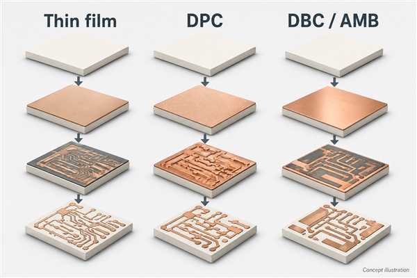
Our ceramic process range includes thin film, thick film, DPC, DBC, AMB, LTCC and HTCC. For Israeli development teams, discussing the metal structure and assembly interface early is more useful than selecting a process from a material name alone.
Protect the Thermal Path Below the Active Device
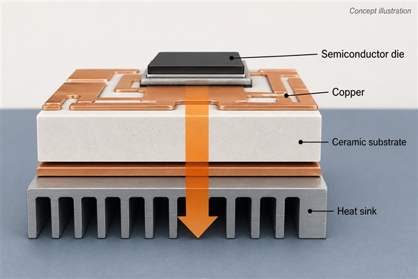
For a laser diode or semiconductor die, a small attachment area can concentrate heat. Aluminum nitride is worth evaluating when conduction through that area limits performance. Alumina may still be appropriate where the heat load and cooling arrangement allow it.
Consider attachment thickness, voiding risk, copper spreading and the final heat-sink interface together. Selecting a higher-conductivity ceramic will not compensate automatically for a poor interface below it. A representative assembled prototype is needed to verify the operating temperature and distribution under the intended duty cycle.
Match Fine Metallization to Device Attachment
Fine-pattern circuits can use thin-film processing or plated routes according to their metal requirements. Our DPC ceramic PCB for sensors are one example of plated circuitry on ceramic; our thin-film ceramic circuits for medical equipment show a different route for compact patterned metallization.
Our thin-film capability includes 20 um minimum line width when film thickness is below 3 um, subject to review of the complete construction. That figure must not be carried over to thick copper. Define attachment-pad finish and usable bonding area together with line geometry so the finished pattern supports the intended soldering or bonding operation.
Use DBC or AMB When the Power Stage Requires Bonded Copper
Our DBC ceramic substrates for IGBT modules include an AlN configuration with 300 um copper. This specific product example illustrates a substantially different conductor structure from a fine-film circuit. Bonded copper can support current distribution and heat spreading where those functions dominate.
For suitable power-module requirements, our AMB ceramic PCBs for power modules provide another bonded-metal route. Ceramic material, copper layout and cycling stress should be evaluated together. A laser-control assembly may use one ceramic construction for the power stage and another for the fine-signal circuitry; there is no requirement to force both onto the same substrate.
Keep Optical, Electrical and Mechanical Interfaces Aligned
A ceramic circuit can meet its electrical design and still be difficult to integrate if its mechanical references do not match the module. Pad position, mounting location and available clearance should be coordinated with the component and housing drawings.
| Interface | Design focus |
|---|---|
| Active device to ceramic | Attachment area, finish and local heat flow. |
| Ceramic to heat sink or housing | Flatness, support and thermal-interface consistency. |
| Signal circuit to controller | Return path, connector access and separation from switching currents. |
| Optical or sensing reference | Repeatable datum and component placement rather than an unspecified overall tolerance. |
Where optical alignment is required, agree the actual assembly scope with our team. Ceramic circuit fabrication alone is not a promise of complete optical-module alignment or testing.
Coordinate FPC and Rigid-Flex Without Loading the Ceramic
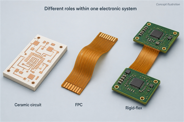
FPC and rigid-flex can reduce routing constraints between a compact module and its surrounding electronics. The flex section should handle the intended movement or installation geometry; the ceramic substrate should remain mechanically supported.
We can review the associated interconnect requirements alongside the ceramic circuit. Keep cable tension and bending forces away from the ceramic joint, and ensure the connector or solder interface can be assembled and inspected. A rigid-flex design still contains rigid component areas, so only its designated flex region should bend.
Validate Laser, Sensor and Medical-Electronics Prototypes
Validation should reflect the module function. A laser driver may need thermal and switching checks; a sensor interface may need signal stability testing. Medical instrumentation also requires attention to the agreed quality documentation and the distinction between a supplied circuit and the finished device.
We align the fabrication and inspection scope with the prototype objectives. Electrical continuity is an important circuit check, but it does not prove optical output, measurement accuracy or finished-device compliance. Keep those system-level acceptance steps explicit when deciding whether a prototype is ready for the next build.
Build a Schedule That Includes the Complete Manufacturing Scope
Ceramic lead time depends on the process, material, metal system, quantity and required inspection. Component sourcing and assembly add separate steps. The date that a bare ceramic circuit is ready is not necessarily the dispatch date for an assembled module.
We confirm project-specific scheduling with the Israeli team and distinguish manufacturing completion from international delivery. If a layout or attachment system is still changing, include a revision decision before recurring production. This keeps schedule expectations connected to the actual technical maturity of the module.
Confirm Current Quality Scope Before Production Release
Quality evidence should identify the manufacturing revision and the inspections applicable to the supplied ceramic circuit. For an assembly, the agreed acceptance requirements must also cover the relevant attachment and component-placement features.
Ask our team for current documentation where ISO 9001 or ISO 13485 evidence is needed. Verify the named entity, covered activity and validity. We do not imply that a circuit-board quality certificate constitutes approval of a laser system, semiconductor module or medical device.
If you need a ceramic PCB manufacturer serving Israel, contact our team at sales@bstceramicpcb.com to discuss your ceramic circuit, prototype build, assembly scope and related FPC or rigid-flex requirements.
 Products
 About us
 Contact us



