






















































 HOME
HOME

-

Ceramic PCB for Humanoid Robot joint actuators
2026 04,07 -
LTCC PCB Surprises: What Most People Miss
2025 12,09 -
Step-by-Step Guide to DPC PCB Design for Sensor Systems
2025 12,03 -
Ceramic PCBs Essential Benefits and Applications
2025 12,01 -
How Al2O3 DPC Ceramic Substrate PCB Enhances Heat Dissipation in Modern Electronics?
2025 11,28 -
How to Choose Between Ceramic, FR4, and Metal Core PCBs
2025 11,27 -
DPC Ceramic PCB Materials: Surprising Science Inside
2025 11,26 -
Wire bondable 2-layer Alumina substrates PCB | Bstceramic PCB
2025 09,22 -
Silicon Nitride Substrate, Silicon Nitride Ceramic Substrate Formula
2025 05,08 -
What is thick film ceramic PCB?
2023 08,02
Custom Ceramic PCB Manufacturer Serving the USA
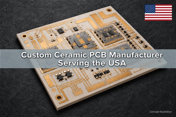
At BSTCeramicPCB, we are a custom ceramic PCB manufacturer serving the USA, manufacturing ceramic circuits in China for US engineering and production teams. Ceramic PCBs for USA semiconductor projects need the copper pattern, die-attachment surface, insulation geometry and assembly process to work together. We support process selection, prototypes and assembly services, and can coordinate related FPC and rigid-flex requirements when the ceramic circuit is part of a larger electronic system.
Manufacturing Support for US Semiconductor Teams
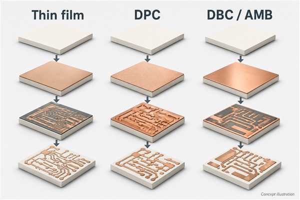
We support ceramic circuit fabrication from the manufacturing review through prototype and production builds. Our ceramic technologies include thick film, thin film, direct plated copper (DPC), direct bonded copper (DBC), active metal brazing (AMB), LTCC and HTCC. These are different process routes, not interchangeable names for the same board.
For a US module developer, the useful starting point is the circuit function: a high-current power substrate needs a different conductor structure from a fine-pitch sensing circuit. We review the substrate, metal system and assembly interface together so that an attractive layout does not become a difficult-to-build part.
DBC and AMB for Power Semiconductor Modules
For high-current modules, bonded copper provides a practical conductor and heat-spreading layer. Our DBC ceramic substrates for IGBT modules include an AlN product example with 300 um copper. That is a specific configuration, not a requirement for every design. Copper thickness and spacing must be selected together because a thicker conductor changes patterning and edge geometry.
Our AMB ceramic PCBs for power modules provide another route for power-module substrates, including designs using silicon nitride. AMB uses an active brazing system to join metal and ceramic; DBC uses a different bonding mechanism. Selection should consider ceramic strength, thermal cycling and the complete attachment stack, rather than treating AMB as an automatic upgrade for every module.
Choose the Ceramic Around the Complete Heat Path
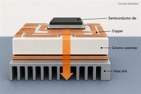
Alumina can suit designs where electrical insulation, mechanical support and cost are the main priorities. Aluminum nitride becomes more attractive when heat flux through a small substrate area is a limiting factor. Silicon nitride deserves consideration where mechanical durability and cycling stress are central to the design.
| Design concern | Manufacturing implication |
|---|---|
| Local hot spot beneath a die | Evaluate substrate thickness, copper spreading and attachment interfaces together. |
| Repeated temperature cycling | Review expansion mismatch, copper balance and ceramic edge condition. |
| High working voltage | Coordinate conductor spacing, substrate insulation and the finished assembly geometry. |
| Compact footprint | Check the actual heat-transfer area before selecting a higher-conductivity material. |
A ceramic substrate does not remove the thermal resistance of solder, sintered attachment or the heat-sink interface. Prototype measurements should evaluate the assembled thermal path, not just a substrate material value.
Sensor and Medical Circuits Need a Different Conductor Strategy
Low-power sensing circuitry often prioritizes pad definition and stable geometry over maximum copper thickness. Our DPC ceramic PCB for sensors are relevant to plated conductor patterns on ceramic. For compact medical instrumentation, thin-film ceramic circuits for medical equipment offer a route to fine metallization on a rigid insulating base.
Keep the sensing node away from large switching-current loops and unnecessary heat sources. In a combined system, the power substrate and sensing circuit may be separate parts with different materials and finishes. We supply the circuit substrate or agreed assembly scope; this does not mean we supply or approve the complete medical device.
Control Fine Features and Assembly Surfaces Together
Manufacturability depends on both the smallest feature and the metal structure around it. Our published thin-film capability includes 20 um minimum line width where the film thickness is below 3 um. This is a process-conditioned capability, not a promise that all materials, metallizations and panel layouts can use that geometry.
Wire bonding, soldering and other attachment methods need compatible surface finishes. Pad finish, flatness, contamination control and the thermal history should be reviewed before production. A fine trace that is fabricable can still be unsuitable for the required current or assembly operation.
Plan Prototype Lead Time Separately from US Delivery
A reliable schedule separates material availability, circuit fabrication, inspection, assembly and international transport. Thin-film patterning, copper bonding and co-fired ceramic processing do not follow the same production sequence, so they should not share an assumed universal lead time.
We confirm the manufacturing schedule against the actual material, geometry, quantity and testing scope. For US deliveries, the dispatch date and arrival estimate should remain separate. Prototype changes, component availability and transport arrangements can each alter the overall plan; an expedited fabrication option does not automatically shorten every downstream stage.
Quality Evidence Must Match the Supplied Part
Quality review should establish what was inspected, which revision was built and which acceptance criteria apply. Dimensional inspection, conductor continuity, insulation checks and agreed assembly inspection have different purposes. A passed continuity test alone does not demonstrate thermal-cycle reliability.
Certification also has a defined legal entity, site, scope and validity period. Discuss current documentation with our team when a project requires ISO 9001 or medical-sector quality-system evidence such as ISO 13485. A sales-scope certificate is not a manufacturing-scope certificate, and neither replaces qualification of the supplied module or finished device.
Combine Ceramic Circuits with FPC and Rigid-Flex
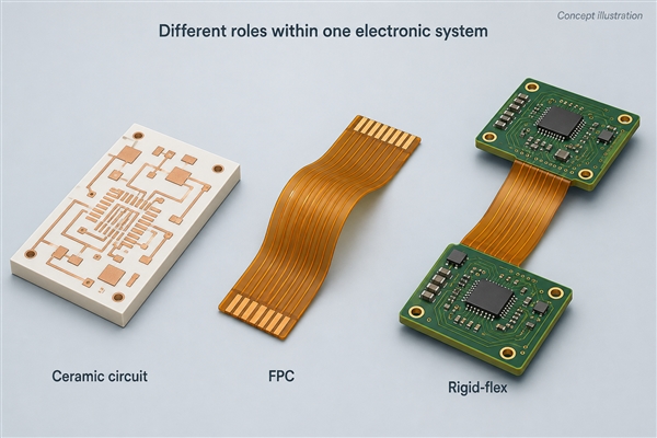
Ceramic, FPC and rigid-flex solve different system problems. Ceramic supports the heat-generating or precision circuit; FPC routes signals through limited space; rigid-flex combines rigid component areas with flexible interconnections. The ceramic portion itself remains rigid.
We can coordinate these related requirements around the ceramic circuit project. Agree the connector or solder interface, mechanical support and assembly order early. Keep bending loads out of the ceramic attachment area, and distinguish an installation bend from repeated flexing. The flex construction and duty cycle determine the appropriate bend design.
Carry the Approved Prototype into Repeat Production
Repeat production should preserve the verified stack, conductor finish and inspection requirements, not only the circuit drawing. A material substitution or attachment change can alter thermal behavior even when the external dimensions stay the same.
Our engineering and production support connects the approved ceramic circuit design with fabrication and assembly planning. For US semiconductor teams, the value is a consistent technical discussion across those stages. Define the changes that require renewed testing before a prototype is released for recurring production.
If you need a ceramic PCB manufacturer serving the USA, contact our team at sales@bstceramicpcb.com to discuss your ceramic circuit, prototype build, assembly scope and related FPC or rigid-flex requirements.
 Products
 About us
 Contact us



