






















































 HOME
HOME

-

Ceramic PCB for Humanoid Robot joint actuators
2026 04,07 -
LTCC PCB Surprises: What Most People Miss
2025 12,09 -
Step-by-Step Guide to DPC PCB Design for Sensor Systems
2025 12,03 -
Ceramic PCBs Essential Benefits and Applications
2025 12,01 -
How Al2O3 DPC Ceramic Substrate PCB Enhances Heat Dissipation in Modern Electronics?
2025 11,28 -
How to Choose Between Ceramic, FR4, and Metal Core PCBs
2025 11,27 -
DPC Ceramic PCB Materials: Surprising Science Inside
2025 11,26 -
Wire bondable 2-layer Alumina substrates PCB | Bstceramic PCB
2025 09,22 -
Silicon Nitride Substrate, Silicon Nitride Ceramic Substrate Formula
2025 05,08 -
What is thick film ceramic PCB?
2023 08,02
What Does Ceramic Pkgs Mean in Electronic Packaging?
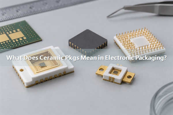
Ceramic pkgs is a shortened search term for ceramic packages used in electronic and semiconductor assemblies. These structures can protect a bare die, route signals and power, provide electrical insulation, and move heat toward the next level of the assembly. In this article, the term does not mean retail packaging for ceramic products or automotive ceramic-coating packages.
What Does Ceramic Pkgs Mean?
Ceramic pkgs means ceramic packages: ceramic-based housings, chip carriers, cavity structures, or package substrates used around semiconductor dies and other sensitive electronic devices. A package may include a ceramic base, patterned conductors, internal vias, external pads or leads, a die cavity, and a lid or seal.
A ceramic package is not the same as a bare ceramic plate. A plate becomes part of a package only after its electrical, mechanical, thermal, and environmental functions are designed into the assembly. Likewise, a ceramic PCB can serve as a package base or interposer, but it is not automatically a complete sealed package.
What Does a Ceramic Package Do?
A ceramic package has four main jobs. It protects the die from handling and the operating environment, connects microscopic die pads to usable external terminals, removes heat, and holds the die in a controlled mechanical position. The importance of each job changes with the device.
- Environmental protection: a properly designed lid and seal can isolate a device from moisture, particles, light, or corrosive media. Ceramic alone does not guarantee hermeticity; the joints, feedthroughs, and seal process determine the finished leak path.
- Electrical interconnection: metallized traces and vias fan out wire-bond or flip-chip connections to leads, lands, pins, or balls.
- Thermal management: the package base carries heat from the die toward a flange, PCB, cold plate, or enclosure.
- Mechanical support: the substrate controls die position, bond-pad geometry, cavity depth, and alignment with optical or RF features.
How Are Ceramic Packages Built?
A typical package starts with a ceramic base or multilayer body. Conductive paste, plated metal, or thin-film metallization forms the internal circuit. Vias connect layers, while a cavity or flat mounting area receives the die. Wire bonding connects top-side die pads to package traces; flip-chip assembly connects bumps directly to package pads.
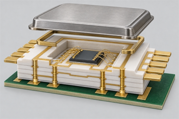
The lid may be metal, ceramic, glass, or an optical window, depending on the device. Soldering, brazing, glass sealing, seam welding, or another qualified process closes the cavity. External interfaces can be pins, gull-wing leads, J-leads, flat leads, lands, or solder balls. These construction choices must be defined together because changing a lid, metallization, or attachment process can change both reliability and electrical performance.
Which Ceramic Materials Are Used in Electronic Packages?
Material selection begins with the required heat path, dielectric behavior, mechanical loading, co-firing process, and cost target. The nominal material name is not enough; grade, thickness, surface condition, and metallization compatibility also matter.
| Material or process family | Why it is used | Important limitation |
|---|---|---|
| Alumina (Al2O3) | Mature electrical insulation, useful mechanical strength, broad metallization compatibility, and comparatively economical processing | Lower thermal conductivity than AlN; the exact grade affects dielectric, thermal, and dimensional behavior |
| Aluminum nitride (AlN) | Higher thermal conductivity with electrical insulation, useful under high heat flux | Higher material and processing cost; handling and metallization need tighter control |
| HTCC | Multilayer ceramic structures with buried conductors and vias for high-temperature, high-reliability package bodies | Conductor choices and shrinkage control are tied to the co-firing system |
| LTCC | Multilayer routing, embedded passive features, and RF-friendly integration at a lower firing temperature | Material system, frequency behavior, layer count, and conductor compatibility must be reviewed as one stack |
Alumina and AlN describe ceramic compositions. HTCC and LTCC describe co-fired material/process systems. Treating all four as interchangeable material labels can lead to an incorrect stack or metallization specification.
What Types of Ceramic Packages Are Common?
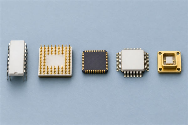
Package names usually describe terminal layout and mounting method, not ceramic composition. Ceramic IC packages therefore need both a package-form designation and a material or construction specification.
| Package family | External connection | Typical design reason |
|---|---|---|
| CERDIP / ceramic DIP | Two rows of through-hole leads | Legacy, military, aerospace, and evaluation devices where robust sealing or temperature range is required |
| PGA | Grid of pins under the body | Higher terminal count with socketed or through-hole attachment |
| LCC / CLCC | Leadless edge lands | Compact surface mounting and a short interconnection path |
| CERQUAD | Gull-wing leads on four sides | Surface-mount fan-out around a ceramic body |
| Ceramic BGA or LGA | Solder balls or flat lands in an area array | High I/O density and a shorter routing path |
| Air-cavity or flange package | Surface-mount leads, lands, or bolt-down flange | RF, microwave, laser, sensor, and high-power devices needing cavity control and a defined heat path |
A “ceramic QFN package” may describe a ceramic leadless package with a QFN-like footprint, but QFN by itself does not mean ceramic. Most commercial QFNs use molded plastic, so the drawing and material callout must identify the actual construction.
Ceramic vs Plastic Packages
The choice is driven by the required environment and qualification level. Plastic is the practical default for most commercial electronics; ceramic earns its cost when the package must support a harsher thermal, moisture, optical, RF, or lifetime requirement.
| Decision factor | Ceramic package | Plastic package |
|---|---|---|
| Environmental seal | Can support a hermetic cavity with compatible metal, glass, or ceramic sealing features | Usually non-hermetic; moisture behavior depends on mold compound and assembly controls |
| Temperature and dimensional stability | Suitable for wide-temperature and high-reliability designs when the full stack is qualified | Adequate for most commercial operating ranges at much lower cost |
| Thermal path | Alumina, AlN, metallized bases, and flanges can be engineered around die heat flow | Thermal performance depends on leadframe, exposed pad, mold compound, and PCB heat spreading |
| RF and optical integration | Supports controlled cavities, feedthroughs, windows, and low-loss interconnect structures | Well suited to volume RF devices when the molded construction meets loss and moisture limits |
| Mechanical behavior | Hard and dimensionally stable but brittle; edge and mounting loads require control | More compliant, but package warpage and moisture sensitivity still require management |
| Cost and availability | Higher tooling, material, metallization, sealing, and inspection cost; fewer standard options | Broad standard-package availability and strong volume economics |
Do not select ceramic solely because it sounds more reliable. Define the failure mechanism first. If a plastic package already meets temperature, moisture, RF, and lifetime requirements, ceramic may add cost without reducing the system risk.
What Design and Assembly Limits Matter?
Package reliability depends on interfaces. The die, attach layer, ceramic, conductors, lid, external terminals, and PCB all expand differently as temperature changes. Large die, stiff joints, thick metal areas, sharp cavity corners, and constrained mounting can concentrate stress in a brittle ceramic body.
- Die attach: specify the attachment material, process temperature, bond-line target, void criteria, and required pad finish.
- Wire bonding: define wire material, pad metallurgy, bond method, loop clearance, and surface cleanliness. A solderable finish is not automatically wire-bondable.
- Flip chip: review bump metallurgy, underfill or cavity condition, coplanarity, pad pitch, and reflow exposure.
- Hermetic sealing: define lid material, seal ring, process, leak-test method, and acceptance level. Hermetic ceramic packages are qualified as assembled structures.
- RF behavior: control dielectric properties, conductor geometry, transition inductance, ground-via placement, cavity modes, and flange contact.
- Board attachment: check terminal finish, land pattern, solder profile, package mass, thermal cycling, and cleaning limits.
Visual inspection alone cannot validate hermeticity, bond strength, RF loss, or thermal-cycle life. The test plan must match the package function and the expected operating environment.
When Are Ceramic Packages Worth the Added Cost?
Ceramic packages are justified when the application needs a combination that a standard molded package cannot economically provide: a qualified hermetic cavity, high die temperature, low-loss RF transitions, an optical window, high heat flux, radiation tolerance, very low outgassing, or long service life in a severe environment.
The main cost drivers are custom tooling, multilayer count, ceramic grade, cavity geometry, via density, metal system, brazed leads or flanges, plating, lid and seal method, inspection level, test documentation, and order quantity. A standard ceramic outline can reduce development cost, while a custom cavity or feedthrough pattern may be necessary when die size, bond-pad layout, RF launch, or thermal path controls the design.
Ceramic is often unnecessary for ordinary consumer and industrial assemblies that already fit a standard plastic package and do not need a hermetic seal, optical access, extreme temperature capability, or a specialized RF/thermal path.
How Do Ceramic PCB Substrates Fit Package-Level Assemblies?
A ceramic PCB substrate can act as a package base, interposer, hybrid-circuit carrier, submount, or the circuit directly beneath a packaged device. It provides patterned conductors on an insulating ceramic, but the complete package may still require die attachment, wire bonding, lead or flange attachment, a cavity lid, and a qualified seal.
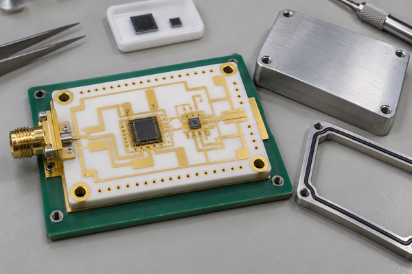
At BSTCeramicPCB, we manufacture ceramic circuit substrates rather than assuming every drawing is a complete package specification. For multilayer routing and buried vias, our HTCC ceramic substrate for high-reliability electronics shows one relevant construction route. A satellite-communication HTCC ceramic substrate is relevant where compact routing and demanding environments meet, while an LTCC ceramic substrate for power-amplifier circuits supports multilayer RF integration.
The substrate drawing should define ceramic system, layer count, finished thickness, cavity and outline dimensions, via structure, conductor material, metallization thickness, surface finish, critical tolerances, attachment method, operating temperature, and required tests. Package-level requirements such as lid sealing and leak testing should be identified separately so responsibility for each operation is clear.
FAQ
Are ceramic packages always hermetic?
No. Ceramic supports hermetic construction, but hermeticity depends on the complete enclosure, feedthroughs, lid, seal process, and leak-test acceptance criteria. An open ceramic substrate or a lidded part without a qualified seal is not automatically hermetic.
Is a ceramic package the same as a ceramic PCB substrate?
No. A ceramic PCB substrate is an insulating ceramic carrying a conductive circuit. It can become the base or interposer inside a package, but a complete package may also include a die cavity, leads, a flange, wire bonds, a lid, and sealing operations.
Why are ceramic packages more expensive?
They use costlier material and forming steps, controlled shrinkage, specialized metallization, brazed or plated features, sealing, and additional inspection. Custom cavities, high layer counts, tight tolerances, low volume, and qualification testing increase the cost further.
Can ceramic packages be surface mounted?
Yes. LCC, CLCC, CERQUAD, ceramic BGA/LGA, leadless cavity packages, and other ceramic semiconductor packages can be designed for surface mounting. The land pattern, coplanarity, finish, solder profile, and thermal-cycle behavior must match the assembly.
Ceramic pkgs are most useful when package-level electrical, thermal, mechanical, or environmental requirements justify ceramic construction. For a ceramic circuit substrate review, send your stack, drawings, metallization requirements, assembly method, and test conditions to sales@bstceramicpcb.com.
 Products
 About us
 Contact us



