






















































 HOME
HOME

-

Ceramic PCB for Humanoid Robot joint actuators
2026 04,07 -
LTCC PCB Surprises: What Most People Miss
2025 12,09 -
Step-by-Step Guide to DPC PCB Design for Sensor Systems
2025 12,03 -
Ceramic PCBs Essential Benefits and Applications
2025 12,01 -
How Al2O3 DPC Ceramic Substrate PCB Enhances Heat Dissipation in Modern Electronics?
2025 11,28 -
How to Choose Between Ceramic, FR4, and Metal Core PCBs
2025 11,27 -
DPC Ceramic PCB Materials: Surprising Science Inside
2025 11,26 -
Wire bondable 2-layer Alumina substrates PCB | Bstceramic PCB
2025 09,22 -
Silicon Nitride Substrate, Silicon Nitride Ceramic Substrate Formula
2025 05,08 -
What is thick film ceramic PCB?
2023 08,02
What Are Ceramic RF PCB Interposer Boards and When Are They Needed?
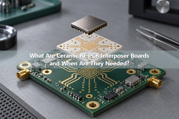
Ceramic RF PCB interposer boards are ceramic circuit structures placed between an RF device or package and a host PCB. They redistribute contacts, shorten or reorganize high-frequency connections, provide controlled ground returns, and create a stable mechanical and thermal interface. The term should not be used for every ceramic RF PCB; the part must actually connect two levels of an electronic assembly.
What Are Ceramic RF PCB Interposer Boards?
Ceramic RF PCB interposer boards are intermediate ceramic circuits that sit between an RFIC, MMIC, module, package, connector, or sensor and the next PCB level. Their conductors and vias fan signals, power, and ground from one footprint to another. The ceramic body also controls spacing, planarity, heat flow, and dimensional stability.
An interposer may be a single-layer alumina plate with thin-film traces, a double-sided AlN circuit with metallized vias, or a multilayer LTCC or HTCC structure. It is different from a passive ceramic spacer because it carries an electrical network. It is also different from a complete RF module because the active devices, shielding, connectors, and enclosure may be assembled elsewhere.
How Does an RF Ceramic Interposer Work?
The signal path normally begins at a wire bond, flip-chip bump, solder land, or compression contact. A patterned transmission line carries the RF signal across the ceramic, while metallized vias or edge grounds connect the return path to the opposite side or internal ground layers. The interposer then launches the signal into the host RF PCB, package, or connector.
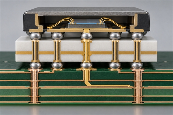
Performance depends on the complete transition, not only the straight trace. Pad capacitance, bond-wire inductance, via geometry, anti-pad size, ground-via spacing, ceramic thickness, solder volume, and the host-board launch all affect return loss and insertion loss. A nominal 50-ohm line can still produce a poor interface if one of these discontinuities is ignored.
Which Ceramic Materials Fit RF Interposer Boards?
Choose the ceramic system from the required frequency behavior, heat flow, routing density, layer count, conductor system, package environment, and cost target. Material grade and process data matter more than a generic ceramic name.
| Material or system | Useful characteristics | Main design limitation |
|---|---|---|
| Alumina (Al2O3) | Mature RF ceramic PCB material, good insulation, dimensional stability, broad thin-film and thick-film compatibility | Lower thermal conductivity than AlN; dielectric data must match the selected purity, frequency, and temperature |
| Aluminum nitride (AlN) | Electrical insulation with a stronger heat path for high-power RF devices | Higher material and processing cost; metallization and handling need tighter process control |
| LTCC | Multilayer routing, buried vias, cavities, ground structures, and possible embedded passive functions | Firing shrinkage, screen-print resolution, material set, and conductor choice constrain the finished geometry |
| HTCC | Robust multilayer ceramic body for demanding temperature and package environments | High firing temperature limits conductor systems and may not deliver the finest or lowest-loss RF routing |
For alumina and AlN ceramic PCB boards, thin film is generally considered when fine surface geometry and controlled conductor definition are important. LTCC becomes more attractive when vertical integration, cavities, buried routing, or compact passive structures matter more than the finest surface line width.
Why Use Ceramic for RF Interposers?
Ceramic is useful when the interface must remain electrically and dimensionally stable across temperature, when the RF device produces concentrated heat, or when short, repeatable transitions are needed within a compact package. A smooth ceramic surface can support fine metallization, while a rigid substrate can maintain pad and bond geometry during assembly.
- High-frequency interconnection: controlled dielectric properties and low-loss conductor systems can support microwave and millimeter-wave routing when the actual material data are used in the model.
- Footprint conversion: the interposer can translate a dense die or package footprint into a pitch the host board can assemble.
- Ground and shielding control: close ground vias, backside metal, cavities, and multilayer grounds can shorten return paths and reduce unwanted coupling.
- Thermal spreading: AlN and metallized ceramic constructions can move heat away from high-power RF devices without creating an electrically conductive base.
- Package integration: ceramic can combine routing, die-attach areas, wire-bond pads, cavities, and external lands in one stable structure.
Ceramic is not automatically the lowest-loss or most economical choice. An organic RF laminate may be better for a large board with moderate temperature exposure, readily available stackups, and no need for fine package-level fan-out.
Ceramic Interposer vs RF PCB vs Package Substrate
The correct name depends on where the circuit sits and which interface it owns. This distinction affects drawings, assembly responsibility, testing, and cost.
| Structure | Primary role | Typical interfaces | When it is the right choice |
|---|---|---|---|
| Ceramic interposer | Redistributes or transitions connections between two assembly levels | Die/package to PCB, module to motherboard, connector to circuit | A footprint, RF launch, thermal path, or mechanical-height transition is required |
| RF ceramic PCB | Carries the functional RF circuit itself | Mounted components, connectors, antennas, filters, bias networks | The circuit can be implemented directly on a ceramic substrate without another interface layer |
| Package substrate | Supports and interconnects a semiconductor die inside a package | Wire bond or flip chip to package terminals | Die fan-out, cavity, lid, seal, or package-level qualification controls the design |
| Host RF PCB | Connects modules and functions across the system | Interposer or package to connectors, power, control, and other circuits | A larger system board can meet the electrical, thermal, and environmental requirements |
One part can perform more than one role, but that must be explicit. Calling a package substrate an interposer does not define who owns die attachment, sealing, or package testing.
What RF Parameters Must Be Controlled?
Use material data for the actual ceramic grade, metallization, frequency, and temperature. A room-temperature nominal dielectric constant is not enough to release an RF interposer for fabrication.
- Dielectric constant and loss tangent: use the supplier's frequency-dependent data in the electromagnetic model and retain the test method.
- Transmission-line geometry: define substrate thickness, conductor thickness, line width, spacing, ground configuration, and whether the structure is microstrip, stripline, or coplanar waveguide.
- Vertical transitions: model signal vias, ground vias, anti-pads, capture pads, via stubs, and the transition into the host PCB.
- Launch and assembly parasitics: include wire bonds, bumps, solder joints, connector pins, and die pads rather than simulating the ceramic trace alone.
- Surface and metal condition: conductor roughness, plating stack, adhesion layer, finish thickness, and bondable or solderable surface requirements affect loss and assembly.
- Coupling and resonances: review cavity dimensions, via fences, ground continuity, nearby lines, and package lids across the full operating band.
The drawing should identify controlled-impedance features and their reference planes. The acceptance plan may use coupons, TDR, S-parameter testing, dimensional inspection, or an assembled test vehicle, depending on frequency and risk.
Which Metallization and Via Processes Fit the Design?
Process selection follows the feature size, metal thickness, layer count, via structure, bond method, and RF loss target. No single ceramic PCB process is best for every interposer.
| Process | Best fit | Watch points |
|---|---|---|
| Thin film | Fine surface traces, precise pads, microwave circuits, wire-bond and flip-chip interfaces | Metal build, adhesion stack, substrate polish, edge coverage, and cost |
| Thick film | Robust printed conductors, moderate feature density, resistors, and economical ceramic circuits | Printed geometry, fired thickness, conductor roughness, paste system, and firing tolerance |
| DPC | Fine patterned copper on alumina or AlN with useful conductor thickness and plated vias | Via aspect ratio, copper stress, flatness, adhesion, and finish compatibility |
| LTCC / HTCC | Multilayer vias, buried routing, cavities, internal grounds, and package-level integration | Layer registration, shrinkage, warpage, via fill, co-fired conductor system, and final surface preparation |
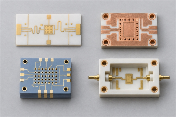
At BSTCeramicPCB, we match the process to the required interconnect rather than treating all ceramic routing as the same. A thin-film ceramic PCB for wireless communication is relevant to fine RF surface routing. An LTCC ceramic substrate for power-amplifier circuits supports multilayer integration, while a thin-film ceramic PCB assembly for radar control is relevant when substrate fabrication and the assembled RF interface must be reviewed together.
What Manufacturing Risks Should Be Checked?
Ceramic interposers concentrate electrical and mechanical requirements into a small part. The most expensive problems usually appear at interfaces, where a drawing leaves one process assumption undefined.
- Warpage and coplanarity: uneven metal, firing shrinkage, substrate size, and copper stress can prevent uniform bump or solder contact.
- Cracks and edge damage: narrow webs, sharp internal corners, large holes, panel handling, singulation, and assembly clamping can load the brittle ceramic.
- Metallization adhesion: the metal system must suit the ceramic surface, thermal cycle, attachment temperature, and required pull or peel test.
- Via defects: incomplete fill, plating voids, misregistration, excessive aspect ratio, and poor ground-via placement can affect both reliability and RF behavior.
- Finish mismatch: wire bonding, soldering, brazing, and conductive adhesive do not use the same ideal surface stack.
- Over-specified tolerances: assigning tight limits to noncritical dimensions raises cost without improving RF performance. Critical transition geometry should receive the tightest control.
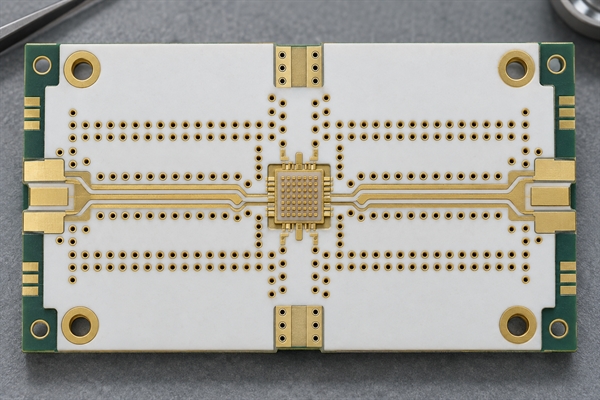
A ceramic PCB prototype should reproduce the intended material, thickness, metal stack, via process, and assembly interface. A simplified coupon is useful for early impedance or adhesion checks, but it does not replace testing the final launch and package geometry.
When Should You Choose a Ceramic RF PCB Interposer?
Choose ceramic RF PCB interposer boards when at least one interface problem cannot be solved cleanly on the device package or host board: very fine fan-out, a short microwave transition, concentrated device heat, a multilayer ceramic cavity, a stable bond platform, or a demanding temperature and reliability environment.
Do not add an interposer only because ceramic has attractive material properties. Every extra interface adds pads, joints, discontinuities, tolerance stack-up, assembly operations, and test requirements. If the RF circuit can connect directly to a qualified host board with acceptable loss, heat flow, pitch, and reliability, the simpler stack is usually easier to manufacture.
What Should a Fabrication Package Include?
A useful fabrication package defines the electrical model and the physical part together. Include the ceramic material and grade, finished thickness, layer stack, conductor and finish stack, outline and cavity dimensions, via type and tolerances, critical line geometry, impedance targets, frequency band, launch reference, attachment method, operating temperature, panel or singulation needs, and inspection or RF test requirements.
Provide native layout data, fabrication drawings, a stack drawing, and a clear distinction between controlled and reference dimensions. For a transition-sensitive design, include the mating package, host-board pad stack, connector or bond geometry, and the simulation reference planes. This prevents a locally correct interposer from failing as part of the complete RF path.
FAQ
Is a ceramic interposer the same as a ceramic PCB?
No. A ceramic interposer is defined by its position between two assembly levels. A ceramic PCB is defined by its ceramic insulating substrate and patterned circuit. A part can be both, but not every ceramic PCB is an interposer.
Can alumina be used for RF interposer boards?
Yes. Alumina is widely used for thin-film and thick-film RF circuits. The design must use dielectric and loss data for the actual alumina grade, frequency, temperature, surface condition, and metallization.
When is AlN preferred over alumina?
AlN is preferred when heat flux is the dominant limitation and electrical insulation is still required. It is usually unnecessary when alumina already meets junction-temperature and reliability targets.
Does a ceramic interposer guarantee 50-ohm impedance?
No. Impedance depends on material properties, substrate thickness, conductor geometry, ground configuration, and the surrounding assembly. The launches, vias, bonds, and solder joints must also be designed and verified.
Can ceramic RF interposers be multilayer?
Yes. LTCC and HTCC can form multilayer ceramic interposers with buried routing, vias, grounds, and cavities. Their shrinkage, registration, conductor system, and RF loss must be considered before the layer structure is released.
Ceramic RF PCB interposer boards are valuable when the interface itself controls RF loss, routing density, heat flow, or package reliability. For an engineering review, send your material, stack, layout, transition geometry, assembly method, and test conditions to sales@bstceramicpcb.com.
 Products
 About us
 Contact us



