






















































 HOME


-

Ceramic PCB for Humanoid Robot joint actuators
2026 04,07 -
LTCC PCB Surprises: What Most People Miss
2025 12,09 -
Step-by-Step Guide to DPC PCB Design for Sensor Systems
2025 12,03 -
Ceramic PCBs Essential Benefits and Applications
2025 12,01 -
How Al2O3 DPC Ceramic Substrate PCB Enhances Heat Dissipation in Modern Electronics?
2025 11,28 -
How to Choose Between Ceramic, FR4, and Metal Core PCBs
2025 11,27 -
DPC Ceramic PCB Materials: Surprising Science Inside
2025 11,26 -
Wire bondable 2-layer Alumina substrates PCB | Bstceramic PCB
2025 09,22 -
Silicon Nitride Substrate, Silicon Nitride Ceramic Substrate Formula
2025 05,08 -
What is thick film ceramic PCB?
2023 08,02
Ceramic Substrate for EV Traction Inverter: How Drive Cycles Shape Module Requirements
Published:
A ceramic substrate for EV traction inverter should be specified from the vehicle mission profile backward. Acceleration, sustained climbing, regenerative braking, repeated urban starts and hot-soak operation create different current, temperature and cycling loads. The useful engineering task is to convert those events into copper, insulation, cooling, geometry and validation requirements that we can manufacture and inspect.
Where Does the Ceramic Substrate Work Inside the Traction Inverter?
The ceramic circuit sits between the power semiconductor interconnects and the baseplate or cooler. Its copper pattern carries switching current and forms die-attach, wire-bond, ribbon or clip areas. The ceramic electrically isolates those conductors while contributing to the heat path from the die to the coolant.
That location makes the substrate a shared electrical, thermal and mechanical component. We manufacture the patterned ceramic circuit to the released package. The inverter team still owns device selection, switching strategy, cooler design and vehicle-level validation, so the drawing must connect those system decisions to measurable substrate requirements.
Which Drive Events Set the Substrate Load Cases?
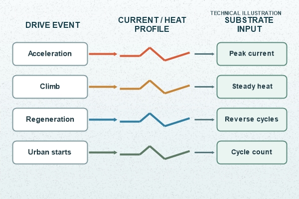
Use the mission profile to define separate load cases instead of one maximum-power number.
| Drive event | Input that must be supplied | Substrate consequence |
|---|---|---|
| Hard acceleration | Peak current, pulse duration, initial temperature | Conductor cross-section and transient temperature rise |
| Sustained grade | Continuous loss, coolant inlet temperature and flow | Steady junction-to-coolant thermal resistance |
| Regenerative braking | Reverse-current level, duration and repetition | Additional electrical and thermo-mechanical cycles |
| Low-speed high torque | Current at reduced vehicle airflow | Cooling performance under an unfavorable boundary |
| Key-on/key-off and urban cycling | Temperature range, dwell and cycle count | Copper-ceramic and attach-interface fatigue exposure |
These are design inputs, not universal EV values. The required profile must come from the target vehicle, inverter controls and cooling architecture.
How Do Semiconductor and Cooling Choices Change the Requirement?
A compact SiC stage and a larger silicon IGBT stage can impose different heat-source footprints, switching-node geometry and local temperature gradients even at a similar inverter rating. Direct liquid cooling, a baseplate-cooled module and a clamped cold-plate assembly also create different lower boundary conditions.
Freeze the die map, die-attach layer, substrate-to-baseplate attach, thermal interface and coolant boundary as one heat path. If an attach layer dominates the thermal resistance, changing only the ceramic may produce little system benefit. If the ceramic is the bottleneck, material and thickness become more influential.
What Requirement Sheet Should Be Frozen Before Material Selection?
Separate the specification into four groups so that one attractive property does not hide another constraint.
- Thermal: loss map, heat-source footprint, coolant boundary and maximum junction target.
- Electrical: DC bus voltage, transient voltage, current paths, proof-test method and partial-discharge requirement when applicable.
- Mechanical: module outline, mounting constraint, functional flatness area, vibration environment and allowed stress.
- Manufacturing: ceramic grade, copper thickness, minimum features, finish, datums and inspection method.
Every limit needs a condition. A voltage without waveform, duration and acceptance criterion, or a flatness value without datum and temperature, cannot be transferred reliably into production inspection.
Which Ceramic-Circuit Route Fits Each Module Job?
For the main traction power stage, DBC and AMB are the primary routes to screen. DBC provides thick copper directly bonded to alumina or aluminum nitride. AMB adds an active-braze interface and is commonly evaluated with silicon nitride when cycling robustness is a dominant concern.
We support an automotive DBC ceramic circuit, an AMB ceramic substrate for IGBT power modules and a DBC ceramic substrate for IGBT semiconductors. The choice depends on thermal resistance, copper geometry, cycling margin, assembly process and cost. Fine-feature DPC circuits may serve auxiliary control or sensing functions, but they should not be presented as a direct replacement for a thick-copper traction power substrate without a specific load case.
How Should Power Layout and Insulation Be Coordinated?
Current paths, switching nodes, gate or sense conductors and edge clearances must be reviewed together. Wide copper reduces conductor resistance, but large islands, abrupt neck-downs and sharp internal corners can raise local stress. Copper-to-edge distance and conductor spacing also interact with encapsulation, contamination and the module's creepage strategy.
Provide current direction, die positions, terminal interfaces, high-dv/dt nodes and keep-out zones with the Gerber or ODB++ data. We can review manufacturable etch compensation, spacing and edge geometry. The inverter designer must approve the electrical loop and insulation coordination for the complete module.
How Should the Complete Thermal Path Be Modeled?
Model heat from the semiconductor junction through die attach, top copper, ceramic, bottom copper, substrate attach, baseplate or cooler and coolant. Use area-specific resistance where spreading is limited; a single bulk conductivity value cannot describe interface coverage, voiding or local hot spots.
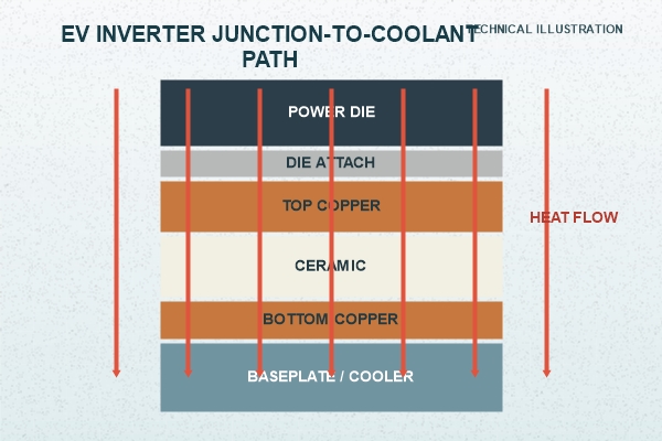
The model should identify which layer controls the result and which uncertainty matters most. That creates a rational prototype plan: measure the uncertain interface instead of changing several materials at once.
What Prototype Matrix Separates Substrate Risk from Module Risk?
Assign each question to evidence at the level where it can actually be answered.
| Question | Recommended evidence | Primary owner |
|---|---|---|
| Does the pattern match the released data? | AOI and dimensional report | BSTCeramicPCB |
| Does the ceramic circuit meet the defined isolation test? | Test method, voltage, duration and result | BSTCeramicPCB or agreed laboratory |
| Is die attach acceptably voided? | X-ray or acoustic inspection after assembly | Module assembler |
| Does the module meet the thermal target? | Instrumented operation under a defined drive event | Module integrator |
| Does the stack survive the mission profile? | Thermal or power cycling plus failure analysis | Shared qualification team |
The matrix prevents a bare-substrate report from being treated as proof of finished-inverter life.
How Should Qualification Evidence Be Assigned and Read Back?
Before testing, define specimen construction, sample quantity, preconditioning, temperature limits, dwell, ramp, failure criterion and analysis method. After testing, connect each failure location to the original load case and drawing characteristic. A center cross-section is not useful if the predicted peak strain is at a copper corner.
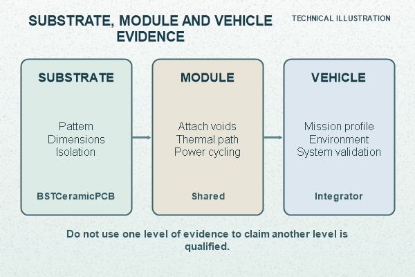
Qualification ownership should also survive design changes. A new die map, copper thickness, finish, attach material or cooler constraint can invalidate only part of the evidence, but that part must be identified before release.
How Do We Convert the System Inputs into a Manufacturable Ceramic Circuit?
We review the released artwork, ceramic and copper construction, finish, datums, tolerances, insulation test and inspection plan as one package. For DCB projects, our current capability list includes up to two layers, a listed minimum board thickness of 0.30 mm and listed minimum line/space of 0.30/0.30 mm; each automotive drawing still requires engineering review. Nickel plating and ENIG are available DCB finish routes when they match the assembly process.
Prototype feedback must become a controlled drawing or inspection-plan revision. We preserve the approved artwork and critical-characteristic records from prototype into production instead of relying on descriptions such as “EV grade” or “high thermal conductivity.”
What Should You Include in the RFQ?
Send the module outline, Gerber or ODB++ files, dimensioned drawing, die map, current and voltage conditions, operating and coolant temperatures, preferred ceramic route, copper thickness, finish, functional flatness area, insulation test, cycling target, prototype quantity and forecast volume. Include the die-attach and substrate-attach processes because they affect finish and interface requirements.
Email the package to sales@bstceramicpcb.com. We will review the manufacturable scope and identify missing inputs before quotation. A ceramic substrate for EV traction inverter is ready to release only when its drawing and acceptance evidence trace back to the actual inverter load cases.
 Products
 About us
 Contact us



