






















































 HOME


-

Ceramic PCB for Humanoid Robot joint actuators
2026 04,07 -
LTCC PCB Surprises: What Most People Miss
2025 12,09 -
Step-by-Step Guide to DPC PCB Design for Sensor Systems
2025 12,03 -
Ceramic PCBs Essential Benefits and Applications
2025 12,01 -
How Al2O3 DPC Ceramic Substrate PCB Enhances Heat Dissipation in Modern Electronics?
2025 11,28 -
How to Choose Between Ceramic, FR4, and Metal Core PCBs
2025 11,27 -
DPC Ceramic PCB Materials: Surprising Science Inside
2025 11,26 -
Wire bondable 2-layer Alumina substrates PCB | Bstceramic PCB
2025 09,22 -
Silicon Nitride Substrate, Silicon Nitride Ceramic Substrate Formula
2025 05,08 -
What is thick film ceramic PCB?
2023 08,02
How Should You Select a Ceramic Substrate for X-Ray Detector Modules?
Published:
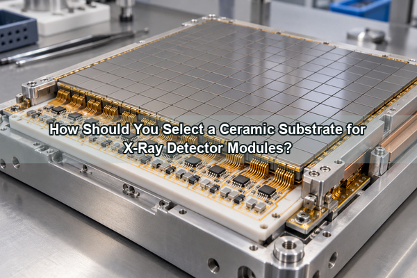
A ceramic substrate for X-ray detector modules provides a rigid, electrically insulating carrier for photodiodes, readout circuits and interconnects while helping control heat, deformation and contamination. It should not be confused with the X-ray conversion material itself: the scintillator or direct-conversion semiconductor performs the radiation-to-signal conversion, while the ceramic circuit supports and connects the detector assembly.
What Does “Ceramic Substrate” Mean in an X-Ray Detector?
In a detector module, ceramic substrate can describe a circuit carrier, interposer or package beneath sensing elements and readout electronics. Its duties can include maintaining flatness, routing low-level signals, supporting flip-chip or wire-bond assembly, providing insulation and carrying heat toward the module frame.
It is different from a ceramic scintillator, X-ray tube ceramic, collimator or shielding material. This distinction must be made before material selection because those parts see different electrical, optical and mechanical requirements.
How Do Indirect and Direct X-Ray Detection Change the Substrate Role?
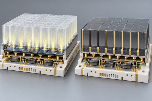
An indirect detector uses a scintillator to convert X-rays into visible light, then photodiodes convert that light into electrical signals. The circuit substrate supports the photodiode array and readout interconnects while preserving alignment with the scintillator structure.
A direct or photon-counting detector converts incident radiation in a semiconductor sensor and sends charge to readout electronics. Its carrier may need dense, repeatable interconnections, stable geometry and controlled parasitics. In either architecture, the ceramic is part of the package and signal path; it is not the sensing medium unless the design explicitly uses a ceramic conversion material.
Which Requirements Should Drive Material Selection?
Choose material from the module loads, not from the application name. Important inputs include detector area, heat generated by the readout ICs, allowable deformation, isolation voltage, operating temperature, mounting method and assembly process.
| Requirement | Substrate question |
|---|---|
| Array alignment | How much local flatness and dimensional stability are required? |
| Readout heat | Is alumina adequate, or is a higher-conductivity material justified? |
| Low-level signals | What dielectric behavior, leakage and routing geometry are acceptable? |
| Assembly stress | How closely must CTE match the detector and package structure? |
| High-speed readout | Are controlled transitions, short returns or multilayer routing needed? |
Alumina is widely used for robust insulating carriers. Aluminum nitride can reduce the ceramic contribution to thermal resistance when readout density or heat flux is higher. LTCC may be considered when multilayer interconnection, cavities or embedded routing is central to the package.
Why Do Rigidity and Flatness Matter?
Large detector arrays can accumulate alignment error across the active area. Substrate deformation can change the relative position of photodiodes, scintillator elements, bump connections or readout ICs. In rotating CT equipment, the module structure can also experience repeated mechanical loading.
Define flatness over the functional mounting or die-attach area, not only across an arbitrary outer outline. The drawing should identify datum features, measurement condition and whether the requirement applies before or after metallization. Polished local areas may be appropriate when flip-chip or thin attach layers require tighter planarity.
How Should Heat from Readout Electronics Be Managed?
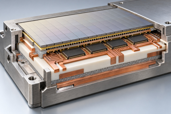
The detector material may generate little heat, while adjacent ASICs, amplifiers and power conditioning create localized loads. Map each heat source and trace the path through attach material, conductor, ceramic, interface and module frame. A high-conductivity substrate cannot compensate for a voided bond line or an undersized contact area.
Our 96% alumina DPC ceramic substrate for sensor circuits is a relevant product reference for a patterned ceramic sensor carrier. The final material and geometry for an X-ray detector must still be based on its heat map and assembly stack.
How Should Low-Level Detector Signals Be Routed?
Detector outputs can be small and sensitive to leakage, coupling and return-path geometry. Separate high-current or switching functions from sensitive analog nodes, keep return paths short, and identify guard structures where the circuit architecture requires them. Routing rules must be developed with the readout IC and module designer rather than copied from a generic digital PCB.
Specify conductor thickness, minimum line/gap, pad geometry, via function and surface finish. For high-speed readout, the substrate dielectric properties, conductor geometry and transition into the next board or connector should be evaluated together.
When Does DPC Fit the Detector Carrier?
DPC is useful when the ceramic carrier needs patterned copper, fine-to-medium circuit features, plated vias or conductors on both faces. It can combine thermal spreading, insulation and interconnection in one rigid part. The process must still match the copper thickness, feature size, via aspect and finish required by the assembly.
When very fine precision metal patterns or wire-bond surfaces dominate, thin-film processing may be a better fit. Our thin-film ceramic circuit for medical equipment is relevant to that manufacturing route. When multilayer cavities or embedded routing dominate, LTCC deserves a separate review.
What Should Be Defined for Pads, Vias and Joining Surfaces?
Each pad needs a declared function: flip-chip bump, die attach, wire bond, soldered component, probe point or connector interface. Finish selection follows that function. “Gold plated” is not enough to establish bondability, solderability or storage performance.
For vias, identify whether they carry signal, ground, current or heat. State the finished diameter, ceramic thickness and required continuity. Keep copper and holes away from cut edges by a process-reviewed margin, especially on thin or narrow ceramic sections.
How Should Cleanliness and Particle Control Be Addressed?
Detector assemblies can be sensitive to contamination near optical paths, fine-pitch joints and high-impedance nodes. Specify cleaning limits that are measurable and relevant to the assembly. Packaging should protect polished surfaces, bonding pads and active-side cleanliness through shipment and handling.
Avoid calling a generic cosmetic requirement “medical cleanliness.” The component drawing should define the actual inspection method, allowable residues, packaging materials and any assembly-specific outgassing or ionic-contamination controls.
What Should the Ceramic Manufacturer Inspect?
A practical substrate acceptance plan can include:
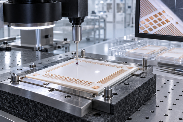
- finished outline, thickness, datum dimensions and local flatness;
- conductor registration, pad dimensions, line/gap and finish condition;
- continuity, isolation and via integrity where applicable;
- surface roughness or polish on functional areas;
- edge chips, cracks, contamination and packaging condition;
- traceability to the approved material and process lot.
Our alumina thick-film ceramic substrate for medical equipment is another same-site product route when printed conductors or resistor functions fit the module. It should be selected by the circuit requirement, not merely because both applications are medical.
What Must Be Validated After Detector Assembly?
The finished module team must validate detector sensitivity, uniformity, noise, image artifacts, thermal drift, calibration stability and mechanical performance under the actual scanner or imaging-system conditions. The ceramic supplier's dimensional and electrical results support that work but do not replace it.
For systems exposed to radiation, the integrator should also define the radiation dose and verify the complete sensor, ASIC, attach, substrate and package stack. A ceramic material name alone does not prove radiation tolerance or medical-device compliance.
How Should the Prototype Represent Production Risk?
Prototype coupons or parts should include the smallest pads, longest sensitive routes, largest copper areas, critical vias, tightest local flatness area and real singulated outline. A simplified test piece that omits the hardest geometry can approve a process without testing the production risk.
Use the same surface finish, cleaning sequence, attach profile and inspection criteria planned for production. If the module architecture changes after the first build, record which acceptance results remain valid and which must be repeated.
What Information Should You Send Us in the RFQ?
Send us the detector architecture, dimensioned substrate drawing, Gerber or ODB++ data, approved ceramic material or required properties, substrate thickness, copper or metal stack, surface finish, vias and critical tolerances. Include detector and readout component footprints, heat map, attach methods, flatness area, cleanliness requirements, inspection plan and prototype/production quantities.
At BSTCeramicPCB, we use these inputs to review the material, circuit process, panel method and inspection scope before quotation. Email the files to sales@bstceramicpcb.com and mark unresolved decisions so they can be reviewed rather than hidden in generic tolerances.
A ceramic substrate for X-ray detector modules succeeds when its role is defined precisely: it supports, connects and stabilizes the detector assembly. Material, routing, flatness, cleanliness and validation should all trace back to that role.
 Products
 About us
 Contact us



