






















































 HOME
HOME


-

Ceramic PCB for Humanoid Robot joint actuators
2026 04,07 -
LTCC PCB Surprises: What Most People Miss
2025 12,09 -
Step-by-Step Guide to DPC PCB Design for Sensor Systems
2025 12,03 -
Ceramic PCBs Essential Benefits and Applications
2025 12,01 -
How Al2O3 DPC Ceramic Substrate PCB Enhances Heat Dissipation in Modern Electronics?
2025 11,28 -
How to Choose Between Ceramic, FR4, and Metal Core PCBs
2025 11,27 -
DPC Ceramic PCB Materials: Surprising Science Inside
2025 11,26 -
Wire bondable 2-layer Alumina substrates PCB | Bstceramic PCB
2025 09,22 -
Silicon Nitride Substrate, Silicon Nitride Ceramic Substrate Formula
2025 05,08 -
What is thick film ceramic PCB?
2023 08,02
Ceramic Substrate: Materials, Metallization, Manufacturing and Applications
Published:
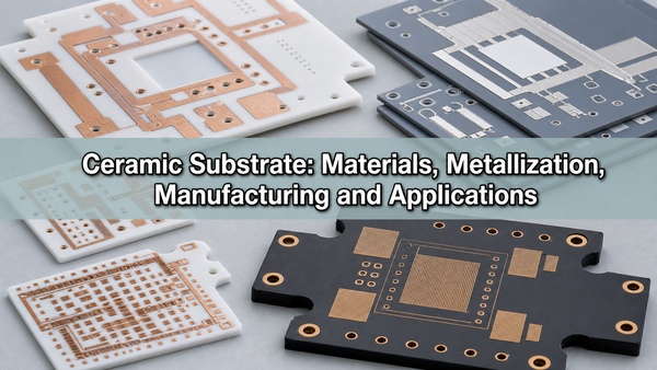
A ceramic substrate is a rigid, electrically insulating base made from an engineering ceramic such as alumina, aluminum nitride, or silicon nitride. In electronic assemblies, it supports conductors and components while providing a stable heat path, high-temperature capability, and dimensional control that organic laminates cannot always maintain. Material grade, substrate thickness, surface condition, and metallization process must be evaluated together because each one changes the finished circuit's thermal, electrical, and mechanical behavior.
What Is a Ceramic Substrate?
A ceramic substrate is a thin structural plate that carries a circuit, semiconductor die, sensor element, heater, electrode, or other functional layer. The ceramic itself is normally an electrical insulator. Heat moves through its solid body, while the patterned metal on the surface carries current or signals. This combination allows the same part to provide mechanical support, dielectric isolation, and thermal conduction.
The term can describe three different product states. A bare substrate is an unmetalized ceramic plate. A metallized substrate adds conductive pads or tracks through printing, sputtering, plating, direct copper bonding, or brazing. A ceramic PCB adds a complete circuit pattern and may include vias, resistors, dielectric layers, surface finishes, and assembled components. Distinguishing these states prevents material properties from being confused with finished-board performance.
What Is a Ceramic Substrate for PCB?
For PCB use, the ceramic replaces the glass-reinforced epoxy core found in FR4. Copper, gold, silver, silver-palladium, or another conductor is attached directly to the ceramic through a process selected for the required line width, copper thickness, current, bonding method, and operating environment. The result may be a single-sided circuit, a double-sided circuit with filled vias, or a multilayer thick-film, LTCC, or HTCC structure.
A ceramic PCB is appropriate when the dielectric layer must tolerate concentrated heat, high voltage, repeated temperature change, low moisture absorption, or a coefficient of thermal expansion closer to semiconductor materials. It is not automatically better for every circuit. Low-power digital assemblies with generous board area usually remain more economical on FR4.
Which Materials Are Used for Ceramic Substrates?
Alumina, aluminum nitride, silicon nitride, and zirconia-toughened alumina cover most electronic substrate requirements. Each material should be identified by grade rather than by chemical name alone because purity, secondary phases, density, and sintering additives change the measured properties.
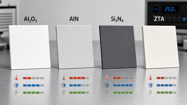
- Alumina (Al2O3): 96% alumina is widely used for thick-film circuits and general electronic insulation. Higher-purity alumina supports cleaner surfaces, improved dielectric behavior, and finer thin-film processing.
- Aluminum nitride (AlN): AlN combines electrical insulation with much higher thermal conductivity than alumina. It is used beneath high-power dies, LEDs, laser devices, and compact power circuits.
- Silicon nitride (Si3N4): Si3N4 provides high fracture toughness and bending strength. It is especially valuable in power modules exposed to severe thermal cycling and mechanical stress.
- ZTA: Zirconia-toughened alumina improves toughness over standard alumina while retaining useful insulation and wear resistance. Its thermal conductivity is lower than AlN, so it is selected for mechanical durability rather than maximum heat spreading.
- BeO and specialty ceramics: Beryllium oxide can provide high thermal conductivity but requires strict controls because inhaled BeO dust is hazardous. Sapphire, quartz, and glass-ceramic materials serve optical, RF, sensing, and hermetic applications.
How Do Al2O3, AlN, Si3N4, and ZTA Compare?
The decision begins with the limiting failure mechanism. A heat-flow limit favors AlN, a thermal-cycling and fracture limit can favor Si3N4, and a balanced general-purpose design often uses alumina. ZTA is considered when impact, wear, or crack resistance matters more than thermal conductivity.
| Material | Typical strength | Thermal behavior | Primary advantage | Common electronic use |
|---|---|---|---|---|
| 96% Al2O3 | Good | Moderate heat conduction | Established processing and cost balance | Thick film, sensors, heaters, general circuits |
| High-purity Al2O3 | Good | Better than lower-purity alumina | Clean surface and stable dielectric properties | Thin film, high-frequency and precision circuits |
| AlN | Moderate | High thermal conductivity | High heat flow with electrical isolation | Power semiconductors, LEDs, laser submounts |
| Si3N4 | High toughness | High thermal-shock capability | Resistance to crack growth and cycling | Automotive and traction power modules |
| ZTA | High toughness | Lower thermal conductivity | Mechanical and wear resistance | Structural insulators and harsh-duty sensors |
Published values are typical, not universal. The correct comparison uses data for the exact grade, thickness, surface finish, and test temperature planned for the circuit.
Which Thermal, Electrical, and Mechanical Properties Matter?
Thermal conductivity determines how readily heat moves through the ceramic, but total junction-to-heatsink resistance also includes substrate thickness, copper spreading, die attach, solder, interface material, and contact area. A thin alumina layer can sometimes produce a lower ceramic-layer resistance than a much thicker high-conductivity material. The basic through-thickness relation is R = t/(kA), where t is thickness, k is thermal conductivity, and A is heat-flow area.
Dielectric constant affects capacitance, impedance, and signal velocity. Dielectric loss matters when AC or RF energy passes through the field. Dielectric strength and volume resistivity determine whether the substrate maintains isolation under voltage and temperature. These parameters are related but cannot replace one another.
Coefficient of thermal expansion influences stress between the ceramic, copper, semiconductor, and solder. Flexural strength, fracture toughness, elastic modulus, edge quality, and residual stress influence handling and thermal-cycling life. A substrate with excellent thermal conductivity can still fail if a sharp internal corner, poor edge finish, excessive copper imbalance, or unsuitable attachment process concentrates stress.
How Are Ceramic Substrates Manufactured?
Most thin electronic substrates are produced by powder processing, forming, firing, and precision finishing. The material manufacturer blends ceramic powder with sintering aids, binders, plasticizers, and solvents. Tape casting forms a controlled green sheet, while dry pressing or other forming methods are used for thicker geometries. Features may be punched or machined before firing when green machining provides a cleaner and more economical route.
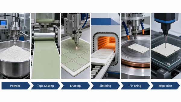
Binder removal and sintering densify the part at high temperature. Shrinkage must be controlled because it changes length, width, thickness, hole position, and flatness. Fired substrates may then be lapped, polished, laser cut, diamond machined, or cleaned. Dimensional inspection, surface roughness measurement, flatness checks, visual inspection, and material-property tests confirm that the substrate is suitable for the next metallization step.
Laser cutting is effective for profiles, slots, and small holes, but energy input can create taper, recast, microcracks, or conductive residue on some materials. Diamond sawing produces straight edges with good control but has a finite kerf and corner-radius limits. Green machining avoids some fired-ceramic cutting difficulty, although final dimensions still depend on predictable sintering shrinkage.
How Are Circuits Metallized on Ceramic Substrates?
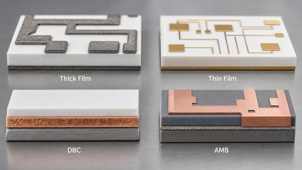
Metallization creates adhesion between a conductor and a chemically stable ceramic surface. Thick-film paste is screen printed and fired. Thin-film systems deposit an adhesion and seed layer by sputtering or evaporation, then define fine features by photolithography and plating. DPC builds copper on a deposited seed layer. DBC bonds copper foil to alumina or AlN through a high-temperature direct-bond process. AMB uses an active braze to join copper to ceramic, commonly Si3N4 or AlN.
The metallization stack may also include nickel, gold, silver, palladium, or other finishes for soldering, aluminum wire bonding, gold wire bonding, corrosion protection, or contact performance. The finish must match the assembly process; a surface optimized for soldering is not automatically optimized for fine gold wire bonding.
How Do Thick Film, Thin Film, DPC, DBC, and AMB Differ?
| Process | Conductor structure | Feature capability | Best fit | Main constraint |
|---|---|---|---|---|
| Thick film | Printed and fired metal paste | Moderate line width; multilayer possible | Hybrid circuits, heaters, sensors, resistors | Paste shrinkage and fired surface geometry |
| Thin film | Deposited adhesion and conductor layers | Fine features and precise geometry | RF, microwave, optical and precision circuits | Thin metal and more process steps |
| DPC | Seed layer plus plated copper | Fine circuits with plated vias | LED, sensors and compact power circuits | Plating uniformity and adhesion control |
| DBC | Thick copper foil directly bonded to ceramic | Power-oriented geometry | IGBT, power conversion and high-current modules | Copper-ceramic stress and etch geometry |
| AMB | Thick copper joined by active-metal braze | Power-oriented geometry | High-reliability Si3N4 and AlN power modules | Braze chemistry, voids and residual stress |
For high-current modules, compare the detailed DBC ceramic substrate structure with an AMB ceramic PCB. The correct process depends on copper thickness, ceramic material, required isolation, thermal cycling, and feature size.
How Do Thickness, Flatness, and Surface Finish Affect Fabrication?
Reducing ceramic thickness lowers through-plane thermal resistance but also reduces stiffness and handling margin. Very thin substrates are more sensitive to edge chips, point loading, copper imbalance, and fixture pressure. Increasing thickness improves rigidity and voltage path length, but it raises thermal resistance and can make laser processing slower.
Flatness controls contact with tooling, screens, photo masks, heatsinks, and assembly fixtures. Warpage can create nonuniform paste print thickness, lithography focus variation, uneven solder joints, or local interface gaps. The flatness requirement should be defined over a stated substrate size because the same percentage or bow limit produces different absolute displacement on a small coupon and a large panel.
Surface roughness affects thin-film continuity, line-edge definition, adhesion, wire bonding, and sealing. Polished surfaces support fine thin-film patterns, while a controlled roughness can improve some mechanical adhesion systems. Excessive roughness can trap chemicals and disturb fine traces; an overly smooth surface can require a more carefully designed adhesion layer.
How Is a Ceramic Substrate Different from FR4 and MCPCB?
FR4 uses glass fiber and epoxy as the structural dielectric. An MCPCB normally uses a metal base, a thin polymer dielectric, and copper circuitry. A ceramic substrate uses the ceramic body itself as the primary dielectric and heat-conducting layer. This removes the polymer dielectric bottleneck found in many metal-core boards, but it also introduces brittle-material machining, edge, and stress constraints.
| Structure | Heat path | Temperature behavior | Mechanical behavior | Typical use |
|---|---|---|---|---|
| FR4 | Low-conductivity organic dielectric | Limited by resin system and Tg | Tough and easy to drill | General digital and low-power electronics |
| MCPCB | Polymer dielectric over metal core | Better heat spreading than FR4 | Robust metal base | LED lighting and moderate-power assemblies |
| Ceramic substrate | Ceramic is the dielectric and heat path | Stable at high temperature | Rigid but brittle | Power, high-voltage, RF and harsh environments |
Where Are Ceramic Substrates Used?
Ceramic substrates are used where electrical isolation, concentrated heat, high temperature, stable geometry, or low moisture absorption is essential. Common assemblies include:
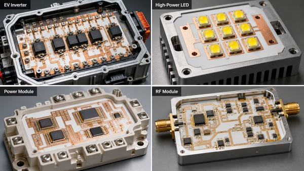
- IGBT, MOSFET, SiC, and GaN power modules for inverters, converters, motor drives, and charging systems;
- high-power LED and laser-diode submounts that require a short electrically isolated heat path;
- hybrid circuits with printed conductors, resistors, heaters, and sensors;
- RF and microwave circuits requiring stable dielectric properties and fine conductor geometry;
- semiconductor packages, chip carriers, and hermetic feedthrough structures;
- medical, aerospace, industrial, and downhole electronics exposed to temperature or chemical stress.
How to Choose a Ceramic Substrate?
Start with the operating limit rather than a preferred material name. Quantify heat flux, maximum junction or surface temperature, isolation voltage, frequency, temperature-cycle range, mechanical loading, and allowable dimensions. Use these conditions to identify the failure mode that the substrate must prevent.
- Select the ceramic grade from thermal conductivity, dielectric behavior, CTE, strength, toughness, and environmental resistance.
- Choose thickness from thermal resistance, voltage path, stiffness, and handling limits.
- Select thick film, thin film, DPC, DBC, AMB, LTCC, or HTCC from conductor thickness, feature size, via structure, current, and assembly method.
- Define surface roughness, flatness, edge condition, hole geometry, and dimensional tolerances that the process can measure consistently.
- Model the complete heat path and stress stack, including copper, die attach, solder, interface material, and heatsink contact.
- Validate the chosen stack with electrical, thermal, adhesion, assembly, and thermal-cycling tests that represent actual service conditions.
FAQ About Ceramic Substrates
Are ceramic substrates semiconductors?
Most alumina, AlN, and Si3N4 electronic substrates are electrical insulators, not semiconductors. They carry semiconductor dies and conductive patterns while maintaining electrical isolation.
What are the main advantages of ceramic substrates?
They combine electrical insulation, higher thermal conductivity than organic laminates, high-temperature stability, low moisture absorption, and dimensional stability. The actual advantage depends on the ceramic grade and metal system.
Can a ceramic substrate have plated through-holes?
Yes. DPC and other metallization processes can form conductive vias, while thick-film and co-fired technologies can also create vertical interconnections. Minimum diameter, aspect ratio, fill quality, and reliability depend on the selected process and substrate thickness.
Can ceramic substrates be laser cut?
Yes. Laser cutting is common for profiles, holes, slots, and scribe lines. The laser type and settings must control taper, recast, residue, heat-affected zones, and microcracking for the selected ceramic.
Is a ceramic substrate always more thermally conductive than an MCPCB?
Not always at the complete assembly level. The result depends on ceramic material and thickness, MCPCB dielectric thickness and conductivity, copper spreading, contact area, and interfaces. Compare total thermal resistance rather than material conductivity alone.
Conclusion
A ceramic substrate should be specified as a complete material-and-process system. Al2O3 provides a proven general-purpose platform, AlN improves heat transfer, Si3N4 improves toughness and cycling capability, and ZTA supports mechanically demanding structures. Thickness, surface finish, flatness, edge quality, and metallization then determine whether those material properties survive in the finished circuit.
BSTCeramicPCB supports ceramic PCB development using alumina, AlN, and other engineered ceramic systems with thick-film, thin-film, DPC, DBC, and AMB process options. For technical support on a ceramic circuit application, contact sales@bstceramicpcb.com.
 Products
 About us
 Contact us



