


 HOME
HOME

-

Ceramic PCB for Humanoid Robot joint actuators
2026 04,07 -
LTCC PCB Surprises: What Most People Miss
2025 12,09 -
Step-by-Step Guide to DPC PCB Design for Sensor Systems
2025 12,03 -
Ceramic PCBs Essential Benefits and Applications
2025 12,01 -
How Al2O3 DPC Ceramic Substrate PCB Enhances Heat Dissipation in Modern Electronics?
2025 11,28 -
How to Choose Between Ceramic, FR4, and Metal Core PCBs
2025 11,27 -
DPC Ceramic PCB Materials: Surprising Science Inside
2025 11,26 -
Wire bondable 2-layer Alumina substrates PCB | Bstceramic PCB
2025 09,22 -
Silicon Nitride Substrate, Silicon Nitride Ceramic Substrate Formula
2025 05,08 -
What is thick film ceramic PCB?
2023 08,02
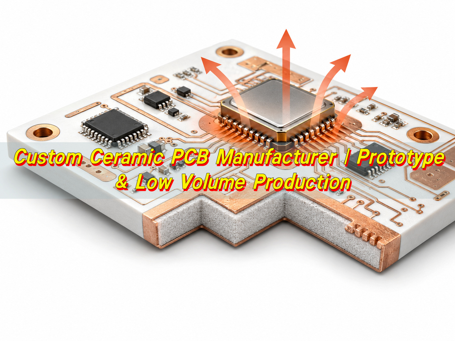
Custom Ceramic PCB Manufacturer | Prototype & Low Volume Production
Ceramic PCBs are used when standard FR4 boards cannot provide enough thermal conductivity, electrical insulation, dimensional stability, or long-term reliability for the application. They are common in power electronics, aerospace modules, medical equipment, RF devices, LED systems, industrial sensors, and automotive electronics. For these projects, the circuit board is more than a carrier for components. It becomes part of the thermal path, insulation system, and mechanical structure.
A qualified ceramic PCB manufacturer helps customers select the right ceramic material, choose the correct manufacturing process, verify design feasibility, and move from prototype to low-volume production with controlled quality. BSTCeramicPCB supports custom ceramic PCB projects using materials such as alumina, aluminum nitride, silicon nitride, LTCC, and HTCC, with process options including DPC, DBC, thick film, and thin film ceramic circuits.
What Is a Ceramic PCB Manufacturer?
A ceramic PCB manufacturer is a specialized circuit board supplier that fabricates printed circuits on ceramic substrates instead of resin-based laminates such as FR4. The substrate may be alumina, aluminum nitride, silicon nitride, LTCC, HTCC, or another engineered ceramic material. These materials provide strong insulation, good thermal stability, low moisture absorption, and reliable performance in demanding operating conditions.
Unlike standard PCB production, ceramic PCB manufacturing requires material-specific processing. Ceramic substrates are hard, dimensionally stable, and less flexible than organic laminates. This means drilling, metallization, copper bonding, plating, firing, cutting, and inspection must be controlled with suitable methods. The manufacturer must understand how ceramic material behavior affects copper adhesion, via structure, solderability, thermal expansion, and board strength.
A ceramic PCB manufacturer is usually selected when the circuit must handle concentrated heat, high voltage, compact packaging, or harsh environments. For example, an aluminum nitride ceramic PCB is often used where heat must move quickly away from power devices. Alumina ceramic PCB is often selected when the design needs a balance of insulation, durability, and cost. LTCC and HTCC are used when multilayer ceramic integration or high-temperature reliability is required.
What Does a Ceramic PCB Manufacturer Do?
A ceramic PCB manufacturer turns a customer’s circuit design into a manufacturable ceramic circuit board. The work starts with engineering review. The manufacturer checks Gerber files, copper thickness, substrate type, hole size, spacing, outline tolerance, surface finish, and application requirements. This review helps confirm whether the design can be produced with stable quality.
After the review, the manufacturer selects or confirms the process route. A DPC ceramic PCB, DBC ceramic substrate, thick film ceramic circuit, thin film ceramic circuit, LTCC module, and HTCC substrate all use different production methods. The right choice depends on thermal performance, current load, circuit precision, mechanical strength, and cost target.
The manufacturer also controls conductor formation. In some designs, copper is plated onto ceramic. In others, copper foil is bonded to the substrate. Thick film circuits use printed conductive paste, while thin film circuits use deposited metal layers for finer features. Each method affects line width, copper thickness, heat spreading, adhesion, and production cost.
Typical services include:
- Design for manufacturability review
- Ceramic material selection
- DPC, DBC, thick film, thin film, LTCC, and HTCC process support
- Prototype and low-volume production
- Surface finish, inspection, electrical testing, and reliability checks
- Assembly support when required by the project
BSTCeramicPCB works with customers from early design review to ceramic PCB production. This helps engineering and purchasing teams confirm material, process, cost, and delivery requirements before starting manufacturing.
What Ceramic PCB Materials Can Manufacturers Provide?
Ceramic PCB materials are selected according to thermal, electrical, mechanical, and cost requirements. The most common materials include alumina, aluminum nitride, silicon nitride, LTCC ceramic, and HTCC ceramic. Each material has a different performance range, so the right choice depends on the application rather than the material name alone.
Alumina is widely used because it offers good insulation, stable mechanical properties, and practical cost control. It is suitable for LED circuits, sensors, industrial electronics, hybrid circuits, and many thick film ceramic PCB designs. Aluminum nitride provides higher thermal conductivity, so it is often used for power modules, laser diodes, RF devices, high-power LEDs, and aerospace electronics. Silicon nitride is valued for mechanical strength and thermal shock resistance, especially in demanding power and automotive applications.
LTCC and HTCC are used for multilayer ceramic circuits. LTCC supports compact integration, RF structures, embedded passives, and small module packaging. HTCC is suitable for high-temperature circuits, hermetic packages, and high-reliability electronic assemblies.
| Ceramic Material | Main Features | Common Applications | Cost Position |
|---|---|---|---|
| Alumina | Good insulation, stable strength, balanced cost | LED, sensors, industrial circuits, thick film circuits | Lower than AlN |
| Aluminum Nitride | High thermal conductivity and good insulation | Power modules, lasers, RF, aerospace, high-power LED | Higher than alumina |
| Silicon Nitride | High mechanical strength and thermal shock resistance | Power modules, automotive electronics, harsh environments | Higher |
| LTCC | Multilayer integration and RF-friendly structure | RF modules, sensors, compact ceramic packages | Medium to high |
| HTCC | High-temperature stability and strong package reliability | Aerospace, hermetic packages, high-temperature electronics | High |
For cost-sensitive designs, alumina is often a practical starting point. For high heat density, aluminum nitride may provide better system performance. For compact multilayer modules, LTCC or HTCC may be more suitable. A ceramic PCB manufacture supplier should help customers compare these options based on real operating conditions.
What Is the Ceramic PCB Manufacturing Process?
The ceramic PCB manufacturing process depends on the chosen material and circuit technology. A DPC ceramic PCB is built differently from a DBC substrate, thick film circuit, thin film circuit, LTCC module, or HTCC ceramic board. Even so, most ceramic PCB projects follow a similar engineering flow: design review, material preparation, circuit formation, finishing, inspection, and packing.
The process begins with file review. The manufacturer checks copper layers, drill data, line width, spacing, substrate thickness, board outline, surface finish, and tolerance requirements. This step is important because ceramic substrates have different processing limits from FR4. Early review helps identify design details that may affect yield, cost, or reliability.
After review, the ceramic substrate is prepared. The material is cleaned, drilled, laser processed, or shaped according to the design. For DPC, the ceramic surface is metallized and copper is built through plating. For DBC, copper foil is bonded directly to ceramic under controlled conditions. For thick film, conductive paste is screen printed and fired. For thin film, metal is deposited and patterned with high precision.
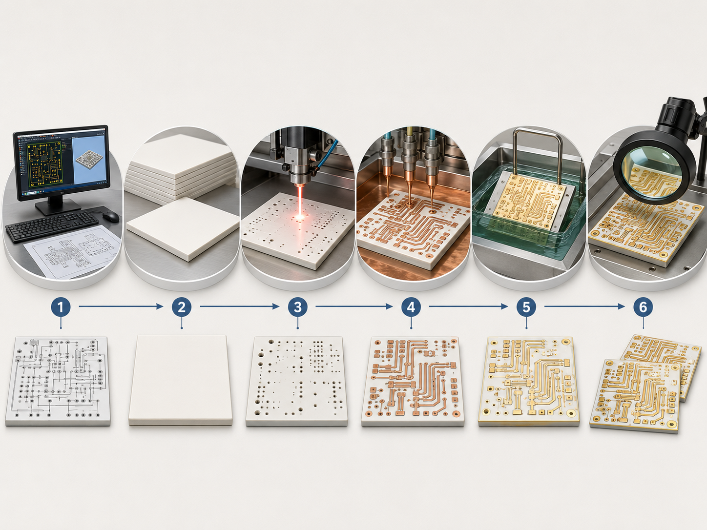
A typical manufacturing flow includes:
- Review Gerber files, drawings, materials, and tolerances
- Prepare and clean the ceramic substrate
- Drill, laser process, or form required holes and outlines
- Build the conductor layer by plating, bonding, printing, or deposition
- Pattern the circuit through etching, firing, or photolithography
- Apply the required surface finish
- Inspect dimensions, copper quality, insulation, solderability, and electrical continuity
Final inspection is a key part of the process. Ceramic boards are often used in high-value assemblies, so manufacturers check both visual quality and functional requirements. For prototype and low-volume production, inspection results also help customers confirm whether the design is ready for the next build.
What Is the Difference Between DPC, DBC, Thick Film, Thin Film, LTCC, and HTCC?
DPC, DBC, thick film, thin film, LTCC, and HTCC are different ceramic PCB manufacturing technologies. They all create circuits on ceramic materials, but they use different methods to form the conductor layer and interconnection structure. The choice affects copper thickness, circuit precision, thermal performance, cost, lead time, and application fit.
DPC, or Direct Plated Copper, is suitable for fine circuits, plated vias, and compact ceramic layouts. DBC, or Direct Bonded Copper, is used where thick copper and strong heat spreading are required. Thick film uses conductive paste printed onto ceramic and fired at high temperature. Thin film uses deposited metal layers and is suitable for precision circuits. LTCC and HTCC use stacked ceramic layers that are co-fired to form multilayer ceramic structures.
| Process | Basic Method | Main Strength | Common Applications |
| DPC | Copper is plated onto metallized ceramic | Fine lines, plated vias, flexible layout | LED, sensors, compact power circuits |
| DBC | Copper foil is bonded directly to ceramic | Thick copper and strong thermal path | IGBT modules, power substrates, EV electronics |
| Thick Film | Conductive paste is printed and fired | Practical for hybrid and resistive circuits | Sensors, power circuits, ceramic base circuits |
| Thin Film | Metal is deposited and patterned | High precision and stable electrical behavior | RF, microwave, medical, precision circuits |
| LTCC | Ceramic layers are printed, stacked, and co-fired | Compact multilayer integration | RF modules, antennas, sensors |
| HTCC | Ceramic layers are co-fired at high temperature | High-temperature and package reliability | Aerospace, hermetic packages, harsh environments |
There is no universal process for all ceramic PCB designs. A power module may require DBC for copper thickness and thermal spreading. A compact LED board may use DPC for plated vias and layout flexibility. A precision RF circuit may require thin film. A multilayer communication module may use LTCC. The correct process should be selected after reviewing the performance target, geometry, quantity, and cost range.
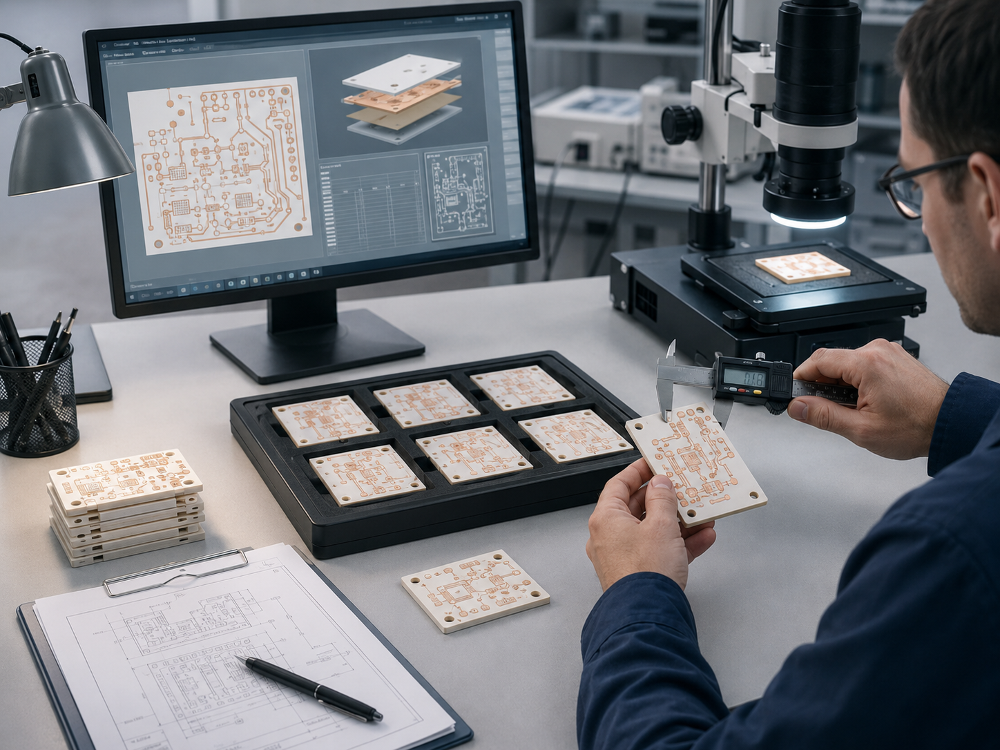
Can a Ceramic PCB Manufacturer Make Prototypes?
Yes. Ceramic PCB prototypes are widely used for design validation before low-volume or larger production. A prototype helps the customer test electrical performance, thermal behavior, component fit, solderability, mechanical assembly, and product-level function. This is useful for power modules, laser systems, RF circuits, aerospace electronics, medical devices, and new product development.
Prototype production also helps confirm material choice. In some cases, alumina provides enough thermal and electrical performance at a controlled cost. In other cases, aluminum nitride is selected because the design has concentrated heat and needs a stronger heat path. A prototype gives the engineering team measured results, which can support better design decisions.
Ceramic PCB prototypes need careful review because the material and process costs are higher than standard FR4. Design details such as narrow ceramic bridges, small holes, heavy copper, tight tolerances, or complex outlines can affect production yield. A qualified ceramic PCB prototype manufacturer checks these details before fabrication and suggests practical changes when needed.
BSTCeramicPCB supports custom ceramic PCB prototype projects by reviewing design files, checking manufacturability, recommending suitable materials, and producing small batches for validation. This helps customers move from concept to tested hardware with clearer technical and cost expectations.
Can a Ceramic PCB Manufacturer Support Low-Volume Production?
Yes. Low-volume ceramic PCB manufacturing is common in industrial, medical, aerospace, automotive, RF, and power electronics projects. Many ceramic PCB designs start with prototypes, then move to pilot runs or small production batches before larger demand is confirmed. A manufacturer that supports low-volume production gives customers flexibility while maintaining process control.
Low-volume production requires more than small-quantity fabrication. The supplier must repeat material selection, copper thickness, surface finish, dimensions, and inspection requirements from batch to batch. This is important when the board is used in high-power modules, sensors, optical devices, or high-reliability equipment.
For low-volume projects, documentation and communication are important. The manufacturer should record the agreed material, thickness, copper structure, finish, tolerance, testing method, and packaging requirements. When a design revision is needed, changes should be reviewed before production so that quality and cost remain controlled.
Low-volume production also gives customers a practical path to market. Engineering teams can test product performance, collect feedback, and improve the design before increasing quantity. Purchasing teams can manage cost and inventory more effectively. BSTCeramicPCB supports low-volume ceramic PCB manufacturing for customers who need stable quality, engineering feedback, and controlled production without unnecessary production scale.
What Applications Need Ceramic PCB Manufacturing Services?
Ceramic PCB manufacturing services are used when the circuit must handle heat, voltage, miniaturization, or operating stress beyond the capability of standard materials. Ceramic substrates are often selected for electronic products where thermal management and stable insulation directly affect performance and service life.
Power electronics is a major application area. DBC ceramic substrates and aluminum nitride ceramic PCBs are used in IGBT modules, MOSFET modules, motor drives, inverters, converters, and EV power systems. These applications benefit from efficient heat transfer and high insulation strength.
High-power LED and laser systems also use ceramic PCBs. Heat is concentrated near the light source, so the substrate must move heat away from the device quickly. Better thermal performance can support stable output, compact structure, and reliable operation.
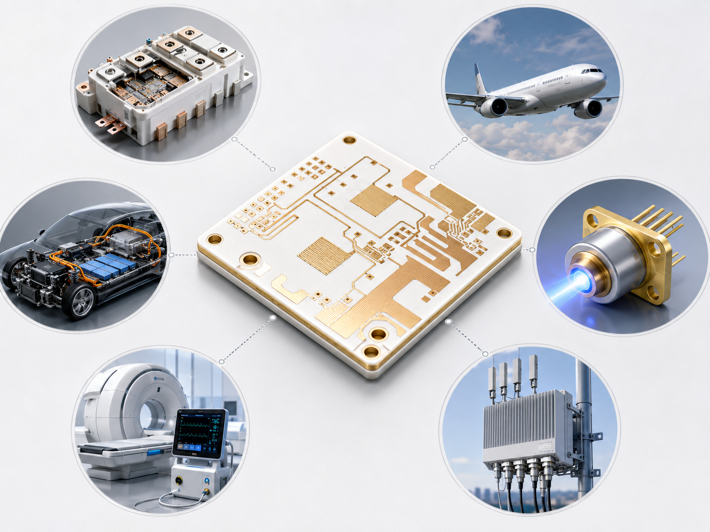
RF and microwave devices use ceramic substrates for stable dielectric behavior, compact layouts, and fine circuit geometry. Thin film ceramic circuits and LTCC modules are common in antennas, communication modules, radar, and microwave devices. Medical and aerospace electronics may use ceramic PCBs because of stability, cleanliness, thermal cycling resistance, and compact packaging needs.
Common applications include:
- Power modules, IGBT substrates, MOSFET modules, and high-current circuits
- High-power LED, UV LED, laser diode, and optical communication modules
- RF, microwave, radar, antenna, and telecom electronics
- Aerospace AlN ceramic PCB boards and avionics modules
- Medical sensors, diagnostic devices, and compact electronic assemblies
- EV power systems, charging modules, industrial controls, and precision sensors
In these applications, the ceramic PCB supports system-level reliability. It helps manage heat, maintain insulation, reduce package size, and improve long-term stability under demanding conditions.
What Factors Affect Ceramic PCB Cost?
Ceramic PCB cost is affected by material, manufacturing process, design complexity, copper thickness, quantity, tolerance, and testing requirements. Because ceramic substrates and ceramic circuit processes are more specialized than standard PCB fabrication, accurate pricing depends on clear technical information.
Material selection has a direct impact. Alumina is usually more cost-effective than aluminum nitride. Aluminum nitride costs more because it offers higher thermal conductivity. Silicon nitride, LTCC, and HTCC may also increase cost because of material properties and process requirements.
The process route also matters. DPC, DBC, thick film, thin film, LTCC, and HTCC have different cost structures. DBC may be selected for thick copper and power modules. Thin film may be selected for high-precision circuits. LTCC and HTCC involve multilayer ceramic processing and firing control. Each process has different equipment, time, yield, and inspection requirements.
| Cost Factor | Why It Matters | Cost Impact |
| Ceramic material | Alumina, AlN, SiN, LTCC, and HTCC have different base costs | Medium to high |
| Substrate thickness | Thickness affects material use, strength, and processing | Medium |
| Copper thickness | Thicker copper supports current and heat spreading but adds process demand | Medium to high |
| Line width and spacing | Fine features require tighter process control | Medium to high |
| Board size and outline | Complex shapes and poor panel use increase waste | Medium |
| Holes and vias | Small holes, plated vias, and special structures add steps | Medium to high |
| Quantity | Setup cost is spread over fewer or more boards | Medium |
| Testing requirements | Extra inspection or reliability testing adds cost and value | Low to high |
Cost should be evaluated together with performance. A lower-cost material may be suitable for many industrial applications. A higher-performance material may reduce thermal stress and improve product reliability. A knowledgeable supplier can help customers select a practical option before production starts.
How Can Ceramic PCB Manufacturing Be More Cost-Effective?
Ceramic PCB manufacturing becomes more cost-effective when material, design, process, and quantity are planned together. The goal is to meet the technical requirement without adding features that do not improve product performance.
Material selection is the first cost-control point. If the design does not require very high thermal conductivity, alumina may provide a strong balance of performance and cost. If the product has a high heat density, aluminum nitride may be worth the higher material cost because it supports better thermal transfer. For compact RF modules, LTCC may reduce assembly complexity by integrating multiple functions into one ceramic structure.
Design optimization is also important. Tight tolerances, fine lines, complex outlines, heavy copper, and special vias can increase cost. These features are useful when the application requires them. When they are not essential, adjusting them can improve yield and reduce manufacturing cost.
Customers can also improve cost control by sending complete files and clear requirements. Thermal targets, voltage level, operating temperature, quantity plan, assembly method, and quality requirements help the manufacturer recommend the right process. For low-volume production, reducing frequent file changes also helps keep cost predictable.
BSTCeramicPCB recommends discussing design intent early. When the manufacturer understands the application, it can suggest suitable materials, standard thickness options, better panel utilization, and practical tolerance choices. This approach helps customers achieve cost-effective ceramic PCB manufacturing without sacrificing the requirements that matter.
What Files Should Customers Send to a Ceramic PCB Manufacturer?
Customers should send complete technical files so the manufacturer can review feasibility, quote accurately, and prepare production correctly. Ceramic PCB projects often involve material and process decisions that depend on details in the design package. Clear files reduce review time and help avoid misunderstandings.
The Gerber file package is essential. It defines copper layers, drill data, board outline, solder mask if used, paste layer, and marking information. A fabrication drawing should also be included. This drawing should show substrate material, substrate thickness, copper thickness, dimensions, tolerances, surface finish, and special notes.
For multilayer ceramic PCB projects, the customer should provide a stack-up drawing. For assembly projects, the BOM, pick-and-place file, assembly drawing, and critical component datasheets are needed. If the board is used in high-power, RF, aerospace, or medical applications, the customer should also provide operating conditions such as current, voltage, frequency, temperature range, thermal target, and reliability requirements.
A complete file package may include:
- Gerber files, drill files, and board outline data
- Fabrication drawing with material, thickness, copper, finish, and tolerances
- Stack-up drawing for multilayer ceramic PCB review
- BOM, pick-and-place file, and assembly drawing if assembly is required
- Critical component datasheets
- Thermal, voltage, frequency, and operating environment requirements
- Testing, inspection, packing, and documentation requirements
Customers can still start a discussion with early design files. However, a complete package allows the manufacturer to provide faster feedback, more accurate pricing, and clearer production advice. BSTCeramicPCB can review files and help identify missing information before ceramic PCB manufacturing begins.
How Do You Choose the Best Ceramic PCB Manufacturer?
Choosing the right ceramic PCB manufacturer means checking whether the supplier can support your material, process, application, quantity, and quality requirements. The decision should be based on technical capability, communication quality, process control, and production consistency.
Start with process capability. A qualified supplier should understand DPC, DBC, thick film, thin film, LTCC, and HTCC technologies. Each process has a different purpose. A power substrate may need DBC. A fine-line ceramic circuit may need DPC or thin film. A compact RF module may need LTCC. The manufacturer should explain which option fits your design and why.
Material knowledge is also important. The supplier should be able to compare alumina, aluminum nitride, silicon nitride, LTCC, and HTCC in practical terms. It should understand thermal conductivity, insulation, copper adhesion, solderability, surface finish, and thermal expansion. For aerospace AlN ceramic PCB board projects, reliability and traceability may be important. For industrial designs, cost control and repeatable quality may be the main focus.
Quality control should be reviewed before ordering. Ask how the supplier checks dimensions, conductor quality, adhesion, electrical continuity, insulation, surface finish, and solderability. For sensitive projects, ask whether inspection reports, traceability, and production records can be provided.
BSTCeramicPCB supports customers looking for a custom ceramic PCB manufacturer, ceramic PCB prototype manufacturer, low-volume ceramic PCB manufacturing partner, and ceramic PCB manufacturing services supplier. The company works with alumina ceramic PCB, aluminum nitride ceramic PCB, DPC ceramic PCB fabrication, DBC ceramic PCB, thick film ceramic PCB, thin film ceramic PCB, LTCC ceramic PCB, and HTCC-related ceramic circuit projects.
In summary, a suitable ceramic PCB partner should help you choose the right material, select the correct process, control cost, review manufacturability, and maintain stable quality from prototype to low-volume production. For custom ceramic PCB manufacturing, prototype support, or small-batch ceramic PCB production, contact BSTCeramicPCB at sales@bstceramicpcb.com
 Products
 About us
 Contact us


