






















































 HOME
HOME

-

Ceramic PCB for Humanoid Robot joint actuators
2026 04,07 -
LTCC PCB Surprises: What Most People Miss
2025 12,09 -
Step-by-Step Guide to DPC PCB Design for Sensor Systems
2025 12,03 -
Ceramic PCBs Essential Benefits and Applications
2025 12,01 -
How Al2O3 DPC Ceramic Substrate PCB Enhances Heat Dissipation in Modern Electronics?
2025 11,28 -
How to Choose Between Ceramic, FR4, and Metal Core PCBs
2025 11,27 -
DPC Ceramic PCB Materials: Surprising Science Inside
2025 11,26 -
Wire bondable 2-layer Alumina substrates PCB | Bstceramic PCB
2025 09,22 -
Silicon Nitride Substrate, Silicon Nitride Ceramic Substrate Formula
2025 05,08 -
What is thick film ceramic PCB?
2023 08,02
DIP-16 Ceramic Package: Dimensions, Construction and PCB Assembly
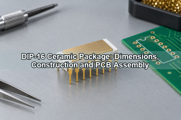
A DIP-16 ceramic package is a 16-lead through-hole enclosure with two parallel rows of eight pins and a ceramic body. It is commonly selected when a device needs a stable package outline, a qualified cavity seal, wide-temperature performance, or a robust platform for die attach and wire bonding. The package name alone does not define every dimension, material, or seal, so the controlling drawing must remain the final reference.
What Is a DIP-16 Ceramic Package?
“DIP” means dual in-line package, and “16” means the package has sixteen external leads. The leads are split into two rows of eight for insertion into plated through holes or a compatible socket. Ceramic versions are often called ceramic DIP, CDIP, CERDIP, or side-brazed DIP, but these names can describe different body and sealing constructions.
A ceramic body does not automatically make the finished component hermetic. Hermetic performance depends on the complete enclosure: ceramic, feedthrough metallization, brazed leads, lid, seal ring, sealing process, and leak-test acceptance criteria.
How Is a Ceramic DIP-16 Constructed?
A typical side-brazed package uses a ceramic base with metallized routing from the die cavity to external lead pads. Leads are brazed to the sides, the semiconductor die is attached inside the cavity, and wire bonds connect die pads to the package conductors. A metal or ceramic lid then closes the cavity.
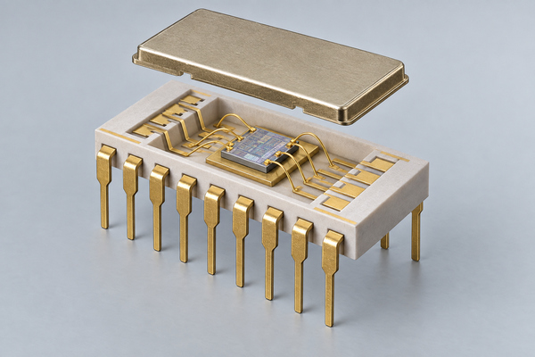
CERDIP construction may use two ceramic sections joined with a glass sealing system, while a side-brazed package generally uses one ceramic body with leads attached around it. These constructions can share a similar PCB footprint but differ in cavity geometry, seal temperature, materials, and reliability qualification.
What Are Typical DIP-16 Package Dimensions?
Many narrow DIP-16 outlines use a 2.54 mm (0.100 inch) lead pitch and a nominal 7.62 mm (0.300 inch) row spacing. One widely used plastic DIP16 reference outline has a body length near 19.25 mm, but ceramic metal-seal drawings can permit different body lengths, widths, heights, lead shapes, and tolerances.
| Dimension | Common reference value | Design note |
|---|---|---|
| Lead count | 16 | Two rows of eight |
| Lead pitch | 2.54 mm | Confirm accumulated pitch tolerance on the package drawing |
| Nominal row spacing | 7.62 mm | Often described as 300 mil; other ceramic DIP widths also exist |
| Body length | About 19-21 mm for many 16-lead outlines | Not universal; use the selected package drawing |
| Mounting method | Through hole or socket | Hole and pad dimensions depend on finished lead geometry |
Do not create a production footprint from a generic DIP16 symbol alone. The body width, shoulder-to-shoulder span, lead thickness, lead-form tolerance, seating plane, and stand-off must come from the exact supplier drawing.
How Do Pin Numbering and Orientation Work?
Viewed from the top, pin numbering normally starts at the pin-1 marker and proceeds counterclockwise. For a 16-pin DIP, one row carries pins 1 through 8 and the opposite row carries pins 9 through 16. A notch, dot, chamfer, or marked corner identifies the orientation.
The PCB footprint should include an unambiguous pin-1 indicator on copper, silkscreen, or assembly documentation. This matters especially when a socket can accept the package in either direction or when the ceramic lid hides the die orientation.
Ceramic DIP-16 vs Plastic DIP-16
The footprint may look similar, but the package choice should follow environmental and qualification requirements rather than appearance.
| Decision factor | Ceramic DIP-16 | Plastic DIP-16 |
|---|---|---|
| Cavity and sealing | Can support a metal, ceramic, or glass-sealed cavity | Molded body is generally non-hermetic |
| Temperature capability | Suitable for wider ranges when the complete package and device are qualified | Adequate for most commercial and industrial electronics |
| Moisture protection | Can provide a qualified hermetic barrier | Depends on molding compound and moisture controls |
| Mechanical behavior | Dimensionally stable but brittle | More compliant and less vulnerable to ceramic edge damage |
| Cost and availability | Higher package, sealing, and inspection cost | Broad availability and lower volume cost |
| Typical reason to select | Aerospace, military, high-reliability, evaluation, harsh-environment, or legacy replacement | General commercial and industrial use |
Ceramic is unnecessary when a standard plastic package already meets temperature, moisture, lifetime, and handling requirements. Its value appears when a specific failure mechanism requires the ceramic construction or sealed cavity.
Open-Cavity vs Sealed Ceramic DIP Packages
An open-cavity ceramic DIP is supplied without a sealed lid so the user can attach a die, make wire bonds, inspect the assembly, and complete sealing. It is useful for custom IC packaging, hybrid circuits, sensor experiments, evaluation devices, and low-volume development.
A sealed package contains a completed device or dummy structure and a closed cavity. When hermeticity is required, define the lid material, seal process, leak-test method, and acceptance level. “Lidded” and “hermetic” are not interchangeable terms.
Which Materials and Metallization Systems Matter?
Alumina is common because it combines electrical insulation, dimensional stability, mature processing, and compatibility with metallization and brazing systems. The external leads may use iron-nickel-cobalt alloys or other controlled-expansion metals, while nickel and gold finishes can support brazing, corrosion protection, die attach, wire bonding, or soldering.
The required finish depends on the next operation. Gold suitable for storage and solder protection is not automatically suitable for wire bonding. Specify pad metallurgy, gold type and thickness, wire material, bond method, solder process, and any high-temperature exposure that occurs before bonding.
How Should the PCB Footprint Be Designed?
Start from the maximum material condition of the finished leads, not only the nominal 2.54 mm grid. The drill, plating allowance, positional tolerance, annular ring, solder fillet, and insertion clearance must work together.
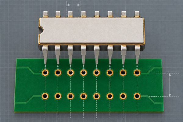
- Set hole size from the actual lead cross-section and its tolerance after plating.
- Keep the two rows aligned to the package drawing's row spacing rather than assuming every ceramic DIP is 300 mil.
- Provide body and lid clearance for sockets, clips, neighboring components, and inspection.
- Use a visible pin-1 mark and verify that the schematic symbol, footprint, assembly drawing, and test fixture use the same numbering.
- Avoid locating fragile ceramic edges against tall components, board stiffeners, or enclosure features.
When interchangeability matters, compare the complete mechanical drawing of every approved package source. Two parts called DIP-16 can share pin pitch but differ in body width, stand-off, lid height, or lead form.
Direct Soldering or an IC Socket?
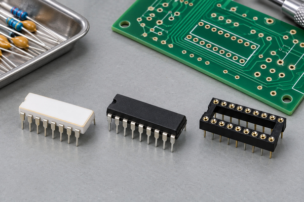
Direct soldering reduces contact interfaces and package height. It is appropriate when the device does not need replacement and the assembly process can control insertion, lead forming, solder temperature, and cleaning.
A socket allows device replacement, protects expensive or programmable parts during prototype work, and reduces repeated soldering on the component. It also adds contact resistance, height, retention risk, and another temperature-rated component. For shock, vibration, or long-life equipment, socket choice and retention need explicit validation.
What Assembly Problems Are Common?
Ceramic packages are hard but brittle. Lead forming too close to the body can load the braze joint or crack the ceramic. Forcing a misaligned package into holes can bend leads and concentrate stress at the package edge. Excessive soldering time can degrade finishes, seals, die attach, or internal bonds even when the ceramic itself tolerates high temperature.
Control the following during assembly:
- lead coplanarity, straightness, insertion force, and bend location;
- solder alloy, flux, preheat, peak temperature, dwell time, and cleaning chemistry;
- board support during manual insertion and rework;
- socket contact finish and insertion-cycle rating, when a socket is used;
- electrostatic discharge controls for the enclosed device;
- visual criteria for chipped ceramic, damaged lid seams, bent leads, and finish contamination.
How Is Reliability Verified?
Testing should match the package function and operating environment. Visual inspection can identify handling damage, but it cannot prove seal integrity, internal bond strength, or thermal-cycle life.
| Risk | Useful verification |
|---|---|
| Cavity leakage | Fine and gross leak testing to the specified acceptance criteria |
| Weak die or lid attachment | Process-qualified shear, pull, or seal-strength test |
| Wire-bond failure | Bond pull or ball/shear testing after relevant thermal exposure |
| Plating or solderability issue | Finish-thickness measurement and representative solderability testing |
| PCB attachment fatigue | Thermal cycling using the actual board, solder, socket, and constraint condition |
| Mechanical damage | Dimensional, lead, lid, and ceramic-body inspection |
Qualification data from a different body size, seal system, or assembly process may not represent the selected DIP-16 package. Keep the test vehicle close to the production construction.
When Should You Choose a DIP-16 Ceramic Package?
Choose this package when the circuit needs a 16-lead through-hole interface and the application benefits from a ceramic cavity, controlled seal, wide-temperature qualification, stable die platform, or compatibility with custom die attach and wire bonding. It also remains relevant for legacy equipment that must preserve a DIP16 board interface.
Use a plastic DIP, surface-mount package, or module when ceramic sealing and package-level customization do not solve a defined requirement. A smaller surface-mount format may reduce board area and interconnect length, while a ceramic LCC, PGA, or custom cavity package may be more appropriate when terminal count or routing density exceeds the DIP format.
How Can Ceramic Circuit Substrates Support Package-Level Designs?
The ceramic package body and the circuit substrate beneath or inside an assembly are related but not identical. BSTCeramicPCB manufactures ceramic circuit substrates; complete die packaging, lid sealing, and hermetic qualification must be defined as separate responsibilities unless specifically included in the project scope.
For multilayer routing and buried conductors, an HTCC ceramic substrate for high-reliability electronics provides a relevant construction route. A satellite-communication HTCC ceramic substrate supports compact routing under demanding environments, while an LTCC ceramic substrate for power-amplifier circuits is relevant to multilayer RF integration.
What Information Should Be Defined Before Manufacturing?
Provide the exact package or substrate drawing, not only the label “DIP-16.” Define body and cavity dimensions, lead pitch and row spacing, lead material and finish, lid and seal method, die size, die-attach process, wire and bonding method, operating temperature, environmental requirement, leak-test criteria, PCB footprint, assembly method, quantity, and qualification plan.
Mark which dimensions are critical to the PCB, socket, die, lid, or test fixture. This prevents a generic outline tolerance from controlling every feature and allows the manufacturer to focus inspection on the interfaces that affect function.
FAQ
Is every DIP-16 ceramic package 300 mil wide?
No. A 7.62 mm (300 mil) row spacing is common for narrow 16-lead DIPs, but ceramic package families can include other widths and body constructions. Use the selected package drawing.
Is the pin pitch always 2.54 mm?
It is the common pitch for standard DIP-16 outlines, but the exact drawing remains authoritative. Verify accumulated pitch, lead width, and positional tolerance before finalizing the PCB.
Can a ceramic DIP-16 be plugged into a plastic DIP-16 socket?
Often yes when the lead pitch, row spacing, lead cross-section, body clearance, and insertion depth match the socket. Do not assume compatibility from pin count alone.
Are ceramic DIP packages still used?
Yes. They remain useful for high-reliability and wide-temperature electronics, legacy replacements, evaluation devices, custom die packaging, and applications requiring a controlled cavity or seal.
Can the ceramic lid be removed and resealed?
Some packages can be opened by a qualified process, but heat and mechanical force can damage the die, wire bonds, seal ring, or ceramic. Resealing requires a controlled procedure and renewed inspection or leak testing.
A DIP-16 ceramic package is defined by more than sixteen pins. The body construction, row spacing, cavity, metallization, lid, seal, lead finish, footprint, and assembly process must work as one system. For a package-level ceramic substrate review, send your drawings, material system, metallization, assembly method, and test requirements to sales@bstceramicpcb.com.
 Products
 About us
 Contact us



