






















































 HOME
HOME

-

Ceramic PCB for Humanoid Robot joint actuators
2026 04,07 -
LTCC PCB Surprises: What Most People Miss
2025 12,09 -
Step-by-Step Guide to DPC PCB Design for Sensor Systems
2025 12,03 -
Ceramic PCBs Essential Benefits and Applications
2025 12,01 -
How Al2O3 DPC Ceramic Substrate PCB Enhances Heat Dissipation in Modern Electronics?
2025 11,28 -
How to Choose Between Ceramic, FR4, and Metal Core PCBs
2025 11,27 -
DPC Ceramic PCB Materials: Surprising Science Inside
2025 11,26 -
Wire bondable 2-layer Alumina substrates PCB | Bstceramic PCB
2025 09,22 -
Silicon Nitride Substrate, Silicon Nitride Ceramic Substrate Formula
2025 05,08 -
What is thick film ceramic PCB?
2023 08,02
What Is Direct Bonded Copper? DBC Substrate Structure and Applications
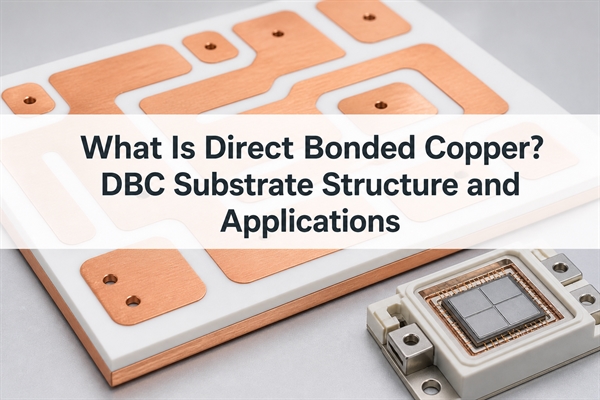
direct bonded copper is a ceramic substrate technology that joins thick copper directly to an electrically insulating ceramic without an organic adhesive layer. The result is a circuit carrier that can conduct high current, spread heat, and isolate power devices from the cooling structure. It is widely used where FR4 or metal-core PCB dielectric layers create too much thermal resistance.
What Is Direct Bonded Copper?
Direct bonded copper, usually abbreviated as DBC or DCB, is produced by bonding pure copper foil to alumina or aluminum nitride ceramic at high temperature. The copper can then be patterned into pads, conductors, and large heat-spreading areas. Unlike a conventional PCB, the ceramic is both the electrical insulation and a structural part of the thermal path.
DBC is appropriate when a design needs thick copper, high isolation, and a short path from semiconductor junctions to a baseplate or heat sink. It is unnecessary for low-power control circuitry that can meet temperature and voltage targets with FR4, insulated metal substrate, or a thinner metallization process.
How Is a DBC Substrate Structured?
A common DBC substrate has copper on both sides of a ceramic tile. The top copper is patterned for the circuit, while the bottom copper improves heat spreading and provides a surface for soldering or sintering the substrate to a baseplate. Single-sided structures are also possible when the mechanical and thermal stack does not require backside copper.
| Layer | Main Function | Design Consequence |
|---|---|---|
| Top copper | Carries current, forms pads, and spreads local heat | Thickness influences ampacity, etching resolution, and stress |
| Ceramic | Provides electrical isolation and transfers heat | Material and thickness control thermal resistance and toughness |
| Bottom copper | Spreads heat and connects the substrate to the cooling stack | Copper balance affects warpage and thermal-cycle stress |
| Surface finish | Protects copper and supports soldering, sintering, or wire bonding | The finish must match the planned assembly process |
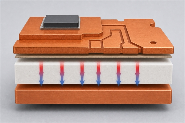
DBC should be evaluated as a complete stack. A high-conductivity ceramic cannot compensate for a thick solder layer, poor interface contact, an undersized baseplate, or an inadequate heat sink.
How Does the Direct Bonded Copper Process Work?
The process uses a controlled copper-oxygen eutectic reaction. A thin oxide condition is created at the copper interface, and the copper-ceramic stack is heated to a narrow temperature region near 1065 C. The eutectic phase wets the oxide ceramic surface and forms a continuous bond as the assembly cools. No polymer adhesive remains between the copper and ceramic.
Alumina presents an oxide surface directly. Aluminum nitride requires controlled surface oxidation before bonding so that a compatible interfacial layer is available. Temperature uniformity, oxygen concentration, surface cleanliness, dwell time, and controlled cooling all affect bond continuity. Excess oxidation can damage copper quality, while insufficient oxidation or contamination can produce voids and weak areas.
After bonding, photoresist defines the circuit pattern and unwanted copper is etched away. Thick copper requires more lateral etch allowance than standard PCB copper. The panel is then inspected, surface finished when required, and separated by laser, diamond cutting, or another ceramic-compatible process.
Which Ceramic Materials Are Used in DBC Substrates?
The main choice is between alumina and aluminum nitride. The correct material depends on heat flux, operating temperature, mechanical loading, insulation requirements, and acceptable cost rather than thermal conductivity alone.
| Ceramic | Typical Thermal Conductivity | Practical Strength | Selection Boundary |
|---|---|---|---|
| Al2O3 alumina | About 20-30 W/mK | Established, economical, and widely available | Good for moderate heat flux where cost and process maturity matter |
| AlN aluminum nitride | About 170-230 W/mK, grade dependent | Lower ceramic thermal resistance and CTE closer to silicon | Useful for concentrated heat sources and high power density |
AlN is not automatically the better purchase. If the ceramic layer contributes only a small part of total thermal resistance, changing from alumina to AlN may add cost without materially reducing junction temperature. A thermal model should identify the dominant resistance before the ceramic grade is upgraded.
What Properties Matter in a DBC Substrate?
| Property | Why It Matters | What to Check |
|---|---|---|
| Thermal conductivity | Controls heat flow through the ceramic layer | Use the actual ceramic grade and operating temperature |
| Dielectric strength | Sets the insulation margin between circuit and cooling structure | Consider ceramic thickness, defects, edge distance, and test method |
| Copper thickness | Affects current capacity and lateral heat spreading | Balance electrical benefit against etching and stress limits |
| CTE compatibility | Drives stress during power and temperature cycling | Review copper pattern, die size, ceramic type, and full module stack |
| Bond integrity | Prevents local thermal resistance and delamination | Define inspection and acceptance for critical interfaces |
| Flatness and warpage | Affect die attach, baseplate contact, and assembly yield | Specify the measurement condition and finished outline |
Direct Bonded Copper vs AMB, DPC, and IMS
The comparison should begin with the required copper thickness, ceramic toughness, feature size, temperature range, and expected thermal cycling. These technologies are not interchangeable versions of the same board.
| Technology | Typical Structure | Main Advantage | When It Is a Better Fit |
|---|---|---|---|
| DBC | Thick copper directly bonded to Al2O3 or AlN | High current, strong heat spreading, and electrical isolation | Power modules, inverters, industrial drives, heaters, and cooling devices |
| AMB | Thick copper actively brazed to ceramic, commonly Si3N4 | High fracture toughness and thermal-cycle reliability | Traction and automotive modules with severe mechanical and thermal cycling |
| DPC | Thin deposited and plated copper on ceramic | Finer features and dimensional precision | LEDs, sensors, RF devices, and circuits that do not need very thick copper |
| IMS | Copper circuit, polymer dielectric, and metal base | Lower cost and familiar PCB processing | Moderate power where polymer dielectric performance is sufficient |
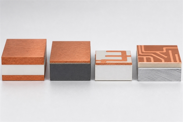
DBC is often the practical middle choice when DPC copper is too thin but the toughness and added process cost of Si3N4 AMB are not required.
How Do Copper Thickness and Circuit Geometry Affect DBC Design?
Thicker copper lowers conductor resistance and improves lateral heat spreading, but it also increases etching time and undercut. As copper thickness rises, minimum conductor width and spacing normally increase. Sharp internal corners, narrow necks beside large copper areas, and abrupt copper-density changes concentrate stress and make dimensional control more difficult.
Designers should keep high-current paths short and wide, use smooth transitions into pads, maintain adequate copper-to-ceramic edge clearance, and balance copper coverage on opposite sides where possible. Copper thickness should be chosen from current density and thermal spreading calculations, not by selecting the maximum available value.
BSTCeramicPCB's published DBC product capability lists conductor thicknesses from 100 to 600 um and a 300/300 um minimum line/space reference. Those values are an initial manufacturing envelope, not a universal guarantee. Actual limits depend on copper thickness, pattern density, ceramic size, finish, tolerances, and inspection requirements.
Where Are Direct Bonded Copper Substrates Used?
DBC is most useful when the same substrate must carry substantial current, isolate high voltage, and conduct heat into a cooling structure.
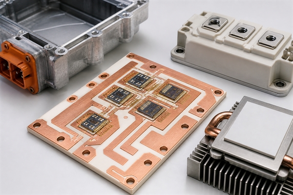
- IGBT and MOSFET power modules: a patterned AlN or alumina substrate supports dies, bond pads, and high-current paths. An AlN DBC substrate for IGBT modules illustrates the thick-copper and high-heat-flux use case.
- Automotive power electronics: inverters, onboard chargers, DC-DC converters, and power distribution assemblies need insulation and controlled thermal expansion. A double-sided DBC ceramic board for automotive components shows how patterned copper and a ceramic core are combined for this environment.
- Cooling and thermoelectric assemblies: large copper areas distribute heat into or away from TECs and cooling structures. This AlN DBC substrate for a portable cooling device is a relevant example.
- Industrial drives and renewable energy: motor drives, solar inverters, wind converters, and solid-state relays use DBC to connect power devices to baseplates.
- High-power LEDs and heaters: DBC can support high current and broad heat-spreading areas when fine DPC features are not the priority.
What Causes DBC Substrate Failures?
| Failure Mode | Typical Cause | Design or Process Control |
|---|---|---|
| Ceramic crack near copper edge | CTE mismatch, sharp corners, or excessive local copper stress | Use rounded transitions, balanced copper, suitable ceramic, and verified thermal cycling |
| Copper-ceramic delamination | Contamination, incomplete eutectic bonding, voids, or repeated cycling | Control surfaces, atmosphere, temperature uniformity, and interface inspection |
| Excessive warpage | Asymmetric copper coverage or unbalanced thickness | Review both sides together and define flatness after finishing |
| Conductor width loss | Undercut during thick-copper etching | Apply the correct etch compensation and avoid unsupported fine geometry |
| Assembly fatigue | Mismatch across die attach, DBC, baseplate, and heat sink | Model the full stack and validate with the intended temperature profile |
| Copper oxidation | Unprotected storage or incompatible thermal processing | Specify finish, packaging, shelf handling, and assembly atmosphere |
Thermal-cycle reliability cannot be judged from peel strength alone. Copper pattern geometry, ceramic toughness, substrate dimensions, baseplate attachment, and temperature swing determine where stress accumulates.
How Should a DBC Design Be Prepared for Manufacturing?
A manufacturable data package should define ceramic material and grade, ceramic thickness, copper thickness on both sides, finished outline, circuit artwork, copper-to-edge clearance, surface finish, flatness, dimensional tolerances, operating temperature, isolation target, and the thermal or power cycling profile. The assembly method also matters because soldering, silver sintering, and wire bonding require different pad finishes and surface conditions.
Critical dimensions should be identified rather than applying the tightest tolerance to every feature. Over-specifying outline, flatness, finish thickness, or cosmetic criteria can reduce yield without improving module performance. Before production, the layout should be checked against the selected copper thickness because a pattern that is practical at 100 um copper may not be practical at 600 um.
FAQ
What is direct bond copper?
Direct bond copper is another common name for DBC. It describes pure copper bonded directly to an oxide-compatible ceramic through a high-temperature copper-oxygen eutectic process.
Is DBC the same as DCB?
In ceramic substrate manufacturing, DBC and DCB are commonly used for the same direct copper bonding technology. Individual suppliers may prefer one abbreviation.
What is bonded copper?
Bonded copper is a broad term for copper joined to another material. In a DBC substrate, it specifically means thick copper metallurgically bonded to ceramic without an organic adhesive layer.
What type of bonding does copper have in DBC?
DBC uses a copper-oxygen eutectic that wets the ceramic's oxide surface and forms a chemical and metallurgical interface during controlled heating and cooling.
Are PCB traces copper or gold?
The electrical conductor is copper. Gold, when present, is normally a thin surface-finish layer over nickel or another barrier layer to protect pads or support a particular assembly process.
Can direct bonded copper use aluminum nitride?
Yes. AlN DBC is used when the ceramic layer must provide much lower thermal resistance than alumina. The AlN surface requires a controlled oxide condition for the bonding reaction.
Is DBC better than AMB?
Neither is universally better. DBC on alumina or AlN often offers a strong cost-performance balance. AMB on Si3N4 is often preferred when fracture toughness and severe thermal-cycle reliability dominate.
How thick is the copper on a DBC substrate?
Commercial DBC commonly uses copper from roughly 0.1 to 0.6 mm, with other constructions available by supplier. The correct thickness depends on current, heat spreading, pattern resolution, and stress.
Can a DBC substrate have vias?
Standard DBC is usually a one- or two-sided ceramic circuit carrier rather than a plated-through multilayer PCB. Ceramic holes and specialized interconnections are possible, but they require process-specific review and should not be assumed to behave like FR4 vias.
Why do DBC substrates crack?
Cracks often begin where copper geometry concentrates stress during temperature changes. Copper and ceramic expand at different rates, so material choice, copper balance, edge geometry, baseplate attachment, and cycling range all affect fatigue life.
Conclusion
direct bonded copper combines thick, patternable copper with a thermally conductive electrical insulator. It is a strong choice for power modules, automotive electronics, industrial converters, cooling assemblies, and other high-current systems, but copper thickness, ceramic material, layout stress, and the complete thermal stack must be evaluated together.
For a practical review of a DBC ceramic substrate design, contact BSTCeramicPCB at sales@bstceramicpcb.com.
 Products
 About us
 Contact us



