






















































 HOME


-

Ceramic PCB for Humanoid Robot joint actuators
2026 04,07 -
LTCC PCB Surprises: What Most People Miss
2025 12,09 -
Step-by-Step Guide to DPC PCB Design for Sensor Systems
2025 12,03 -
Ceramic PCBs Essential Benefits and Applications
2025 12,01 -
How Al2O3 DPC Ceramic Substrate PCB Enhances Heat Dissipation in Modern Electronics?
2025 11,28 -
How to Choose Between Ceramic, FR4, and Metal Core PCBs
2025 11,27 -
DPC Ceramic PCB Materials: Surprising Science Inside
2025 11,26 -
Wire bondable 2-layer Alumina substrates PCB | Bstceramic PCB
2025 09,22 -
Silicon Nitride Substrate, Silicon Nitride Ceramic Substrate Formula
2025 05,08 -
What is thick film ceramic PCB?
2023 08,02
How Should You Specify a DPC Ceramic PCB for Medical Laser Diode Assemblies?
Published:
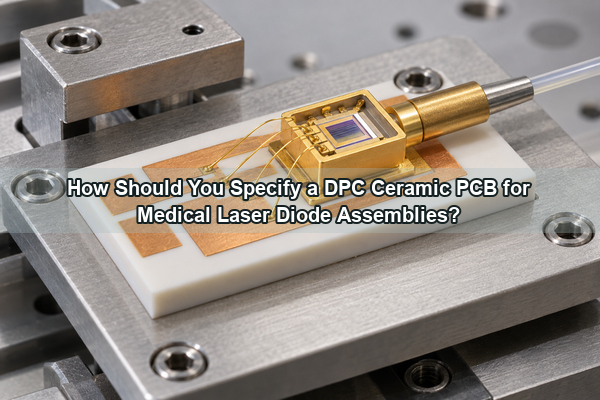
A DPC ceramic PCB for medical laser diode assemblies must carry current, isolate conductors and move concentrated heat away from the laser die without disturbing the optical or bonding geometry. It is a custom ceramic circuit inside the source package, not a complete medical laser and not evidence that the finished device has passed medical certification.
What Does the DPC Ceramic PCB Do in a Medical Laser Diode Assembly?
The ceramic circuit provides a defined mechanical seat for the laser diode, patterned conductors for power and sensing, electrical insulation from the package base and a thermal path toward the cooler or heat spreader. Depending on the package, it may also carry a thermistor, monitor photodiode, polarity marks, wire-bond pads or plated vias.
The word medical describes the end equipment and its validation obligations. The PCB manufacturer still needs a component drawing with electrical, thermal, mechanical and assembly requirements. A surgical source, diagnostic light source and therapy module can use different wavelengths, drive profiles and package boundaries even when the ceramic process is similar.
Which Laser Diode Inputs Must Be Known Before Layout Starts?
Start with the die or packaged-emitter geometry, electrical polarity, optical-axis keep-out, heat-source area and operating waveform. For pulsed operation, provide pulse width, repetition rate, duty cycle and peak current separately from average power. For continuous-wave operation, provide the steady thermal load and cooler boundary.
Assembly inputs are equally important: die-attach alloy or adhesive, maximum process temperature, wire material, bond direction, tool clearance and whether the submount is soldered, clamped or bonded to the next heat spreader. Without these inputs, a visually correct pad layout can still be thermally or mechanically wrong.
Why Use DPC Instead of an Unpatterned Ceramic Plate?
Direct plated copper creates patterned conductors and can support plated interconnections on a ceramic base. This makes DPC useful when the submount needs more than one large metal pad: controlled current paths, isolation gaps, double-sided routing, sensor connections or compact pads can be incorporated into one ceramic circuit.
Our laser-equipment DPC ceramic circuit shows the relevant patterned-ceramic manufacturing route. Its published geometry is not a universal medical laser design; the finished copper, material and surface finish must follow the customer's assembly drawing.
Should the Ceramic Be AlN or Alumina?
Aluminum nitride is often selected when heat flux is high and the ceramic is a meaningful part of the thermal bottleneck. Alumina can be appropriate when the thermal load is lower, cost is more sensitive or the mechanical and metallization process is already established. The correct choice comes from the complete thermal and assembly model, not from one conductivity number.
| Design input | Why it matters to material selection |
|---|---|
| Heat-source area and power profile | Defines local heat flux rather than only total watts |
| Ceramic thickness and footprint | Changes through-thickness and spreading resistance |
| Die-attach and lower interface | Voids and bond-line thickness can dominate the path |
| Package base and cooler | Determines where heat can actually leave the ceramic |
| Thermal-cycle range | Influences stress among die, copper, ceramic and base |
For high-heat designs, our double-sided AlN DPC ceramic circuit is a relevant product reference. We still confirm the actual AlN grade, thickness and conductor construction for each drawing.
How Should the Thermal Path Be Defined?
List every layer from the junction to the coolant or ambient boundary: die, attach layer, top metal, ceramic, lower metal, interface material, package base and cooler. Record thickness, contact area and material for each layer. This prevents bulk ceramic conductivity from being mistaken for total package thermal resistance.
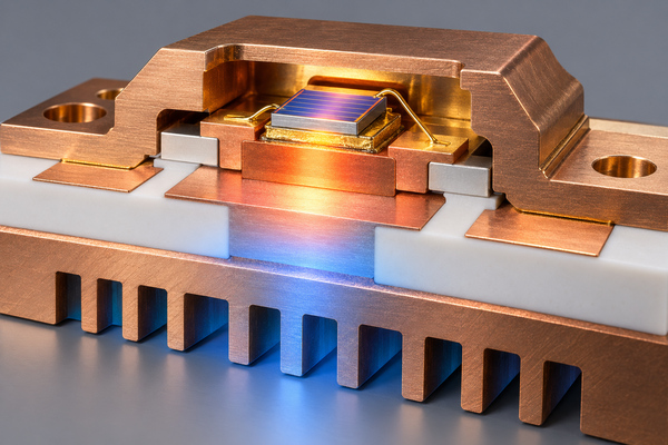
Local spreading also matters. A narrow metal area beneath a high-power emitter constricts heat before it reaches the full ceramic footprint. Conversely, expanding copper without checking stress and optical clearances can create a different problem. Prototype temperature measurements should use the same drive waveform, mounting pressure and cooling condition assumed by the model.
How Should Copper Geometry and Isolation Be Designed?
Define finished copper thickness, minimum line and gap, isolation distance, copper-to-edge distance and current path. Keep the high-current path short and wide where practical, but preserve wire-bond access, optical clearance and inspection visibility. The drawing should identify which pads are electrical returns, die-attach areas, sensor connections and probe points.
If plated vias are required, specify finished hole diameter, ceramic thickness, current function and continuity test. A via used as a signal return has different design priorities from a via intended mainly for heat transfer. Do not copy an organic PCB via rule into a brittle ceramic part without a process review.
What Metallization and Surface Finish Does Assembly Need?
The metal stack must adhere to the ceramic, carry the required current and remain compatible with die attach and wire bonding. “Gold finish” alone is incomplete. State the base conductor, barrier layer, top finish, thickness range and intended joining method.
When the assembly prioritizes very fine metallization, controlled thin-film features or a different bonding surface rather than DPC copper buildup, our thin-film ceramic circuit for medical equipment is a relevant process alternative. We compare the required pad geometry, current load, attachment method and production volume before selecting the metallization route.
For AuSn, indium, solder or conductive adhesive, define the mating metallization and thermal profile. For wire bonding, define gold or aluminum wire, ball or wedge bonding, pad dimensions and the acceptance test. One pad should not be assumed to support soldering, eutectic attach and wire bonding equally well without a verified stack.
How Do Flatness, Roughness and Edge Quality Affect the Package?
Flatness controls bond-line uniformity and contact with the package base. Surface roughness influences metallization continuity, wetting and thin attach layers. Edge chips can remove support or approach active copper on a small submount.
Specify the datum, measured area, part condition and method for each limit. A flatness value measured on bare ceramic is not automatically the same after copper plating or singulation. Critical pad coplanarity may deserve a local requirement rather than an unnecessarily tight limit over the entire outline.
What Changes Between Pulsed and Continuous-Wave Operation?
Continuous-wave operation emphasizes steady-state thermal resistance and cooler capacity. Pulsed operation can create high local temperature excursions and repeated stress even when average power looks modest. The two cases may need different models, copper distribution and qualification profiles.
Do not validate a pulsed design with only an average-power bench test. Likewise, a short pulse test cannot prove that a continuous-wave package reaches an acceptable steady temperature. Record the real electrical waveform and the temperature or optical parameter used as the acceptance endpoint.
How Is a DPC Laser-Diode Ceramic Circuit Manufactured?
A typical route prepares the ceramic surface, forms a seed or adhesion layer, patterns the circuit, builds copper by plating, strips unwanted seed material, applies the specified finish and separates the parts. Double-sided designs add alignment and via-metallization controls. The exact sequence depends on material, copper thickness, via structure and finish.
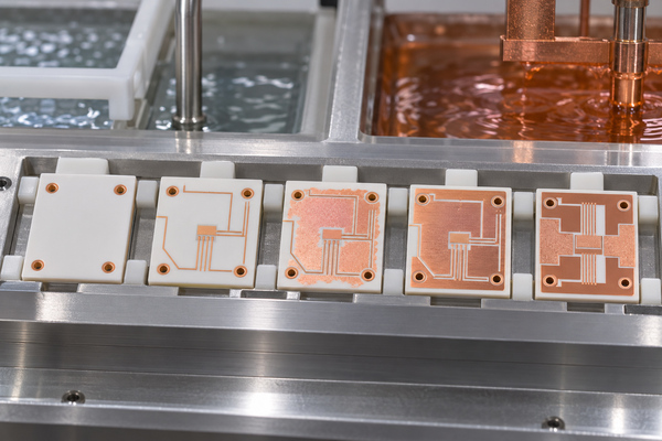
At BSTCeramicPCB, we review the ceramic grade, outline, finished copper, via structure, finish and singulation together. We do not select the process from the words “medical laser” alone. The manufacturing plan must support the customer's die-attach and package process.
What Should Inspection and Prototype Validation Cover?
Inspection should connect each risk to a method rather than rely on one microscope image.
- outline, thickness, local flatness and edge-chip limits;
- conductor registration, line/gap, pad dimensions and copper thickness;
- via continuity and electrical isolation where applicable;
- finish thickness, surface condition and cleanliness;
- representative die-attach coverage, voiding and shear or pull tests;
- thermal response under the intended pulse or continuous-wave condition.
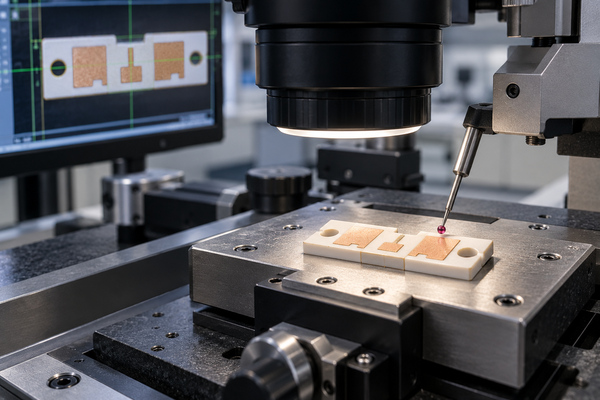
The ceramic supplier can verify the manufactured circuit. The laser-module integrator must still verify optical alignment, output stability, package sealing, cooling controls and lifetime at the assembled-module level.
What Remains a Medical-System Responsibility?
The ceramic circuit does not establish electrical safety, optical safety, software control, risk management, sterilization compatibility or regulatory approval of the final medical device. Those responsibilities remain with the finished-device manufacturer and depend on the intended use and market.
Keeping this boundary explicit improves the RFQ. It allows us to focus the ceramic acceptance plan on dimensions, conductors, insulation, surfaces and traceability while the customer defines the module- and system-level validation that the component must support.
What Should You Send for a DPC Ceramic PCB RFQ?
Send Gerber or ODB++ data, a dimensioned drawing, ceramic material or required properties, finished thickness, copper thickness, finish, vias, critical tolerances and quantity. Add the laser-diode footprint, heat-source area, operating waveform, die-attach process, wire-bond method, cooler boundary and inspection requirements.
If some items are still open, identify them as design decisions rather than filling the drawing with generic limits. We can then review the manufacturable options and quote the defined scope. Email the package to sales@bstceramicpcb.com.
A DPC ceramic PCB for medical laser diode assemblies is most reliable when its material, copper pattern, joining surfaces and acceptance tests are designed around the actual emitter and package. That is the information needed to move from a ceramic concept to a repeatable component.
 Products
 About us
 Contact us



