






















































 HOME


-

Ceramic PCB for Humanoid Robot joint actuators
2026 04,07 -
LTCC PCB Surprises: What Most People Miss
2025 12,09 -
Step-by-Step Guide to DPC PCB Design for Sensor Systems
2025 12,03 -
Ceramic PCBs Essential Benefits and Applications
2025 12,01 -
How Al2O3 DPC Ceramic Substrate PCB Enhances Heat Dissipation in Modern Electronics?
2025 11,28 -
How to Choose Between Ceramic, FR4, and Metal Core PCBs
2025 11,27 -
DPC Ceramic PCB Materials: Surprising Science Inside
2025 11,26 -
Wire bondable 2-layer Alumina substrates PCB | Bstceramic PCB
2025 09,22 -
Silicon Nitride Substrate, Silicon Nitride Ceramic Substrate Formula
2025 05,08 -
What is thick film ceramic PCB?
2023 08,02
How Should You Design a DPC Substrate for Detector Module Integration?
Published:
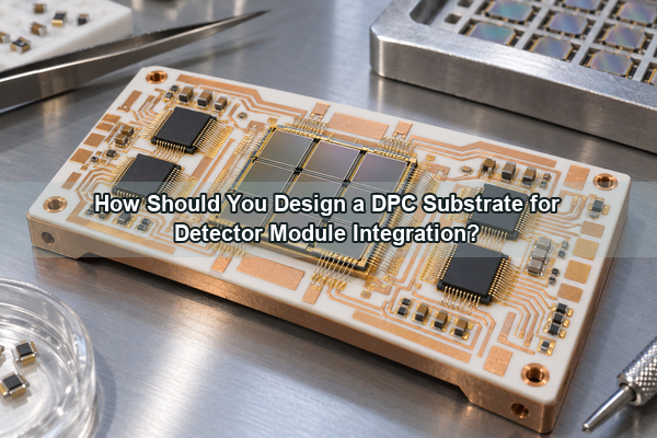
A DPC substrate for detector module integration combines a rigid ceramic base with patterned copper for sensing, power, grounding and thermal transfer. The design should begin with the detector and readout architecture, because the same DPC process can serve optical, thermal, radiation or industrial sensor modules with very different signal and assembly risks.
What Is a DPC Substrate for a Detector Module?
DPC means direct plated copper. A metal seed or adhesion system is patterned on a ceramic base and copper is built to the required circuit thickness. The result can include fine conductor geometry, pads, plated vias and conductors on one or both faces.
In a detector module, the substrate may carry a sensor die, readout IC, thermistor, bias network or connector transition. It is not the detector element itself unless the customer's architecture explicitly makes it part of the sensing mechanism.
Which Module Inputs Must Be Frozen Before DFM?
Provide the detector type, active-area geometry, readout topology, supply and bias voltages, signal levels, heat sources, package outline and mechanical datum scheme. Identify which components are bare die and which are packaged devices. Include wire-bond, flip-chip, solder or adhesive assembly requirements.
The operating environment should cover temperature range, thermal cycling, shock or vibration, humidity or sealing boundary, and any radiation or optical exposure relevant to the completed module. These inputs determine which ceramic, copper structure and inspection plan are meaningful.
Why Is DPC Useful for Detector Interconnects?
DPC can place patterned copper and vias on a ceramic that offers electrical insulation, rigidity and useful thermal performance. This is valuable when a detector module needs a short path from the sensing element to the first-stage electronics or when heat must leave a compact readout region.
Our 96% alumina DPC ceramic substrate for sensor circuits demonstrates the relevant sensor-oriented manufacturing route. The module designer still needs to define its own pad pitch, signal return, copper thickness and acceptance limits.
How Should Alumina and AlN Be Compared?
Alumina is a practical choice for many detector carriers because it provides insulation, rigidity and established metallization options. AlN deserves consideration when local heat flux is higher or the ceramic is a significant part of the thermal bottleneck. The correct comparison includes cost, thickness, surface condition, CTE, thermal cycling and process availability.
| Decision condition | Likely direction |
|---|---|
| Moderate heat, established assembly, cost sensitivity | Start with alumina |
| High readout density or concentrated heat | Evaluate AlN |
| Multilayer routing or cavities dominate | Evaluate LTCC separately |
| Fine precision metal stack dominates | Evaluate thin film separately |
Our double-sided AlN DPC ceramic circuit is a relevant reference when the module needs AlN plus conductors on both faces. It is not a default detector stack.
How Should Sensitive Signals and Grounding Be Organized?
Separate sensitive detector outputs from switching power, clocks and high-current paths. Keep the first-stage return path short and predictable, and identify the reference plane or guard geometry needed by the readout circuit. A DPC substrate can provide ground vias and double-sided structures, but their spacing and inductance must be evaluated for the actual frequency and signal level.
Do not describe every copper area as “ground.” The drawing should distinguish chassis or shield reference, analog return, digital return, bias return and thermal copper where the architecture requires separation. Join points should follow the system grounding plan.
What Must Be Specified for Copper and Vias?
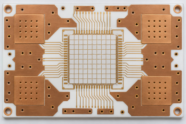
State finished copper thickness, minimum line and gap, pad dimensions, copper-to-edge distance and allowed copper imbalance. For each via, state finished diameter, plating requirement and electrical or thermal function. A via array used as a ground transition should not be accepted only by visual hole count.
The allowable geometry depends on ceramic thickness, copper build and via structure. Narrow gaps next to large copper fields can plate differently from isolated features, so the DFM review should evaluate pattern-density effects rather than treat every location as identical.
How Should Pads and Surface Finish Match Assembly?
Pads should be assigned to wire bonding, flip-chip, soldering, conductive adhesive, probing or connector attachment. Select the metal stack and top finish for that declared use. Gold color does not prove wire-bond quality, and a solderable finish is not automatically suitable for die attach.
Provide wire material and diameter, bonding method, bump or solder alloy, reflow profile and maximum assembly temperature. If the same substrate uses more than one joining method, identify which pads need which finish and whether selective processing is required.
How Should the Thermal Interface Be Designed?
Map detector and readout heat separately. Some detectors generate little heat while the nearby ASIC or bias network creates a local hotspot. The heat path includes attach material, copper, ceramic, lower interface and module frame; a high-conductivity ceramic cannot repair a poor interface.
Use local temperature and thermal resistance targets that can be tested on the representative assembly. If the substrate is clamped, specify support and contact pressure. If it is soldered, define the lower metallization and void criteria.
How Do Flatness, CTE and Mechanical Support Interact?
Flatness affects die attach, bump coplanarity and contact with the module base. CTE mismatch among the detector die, copper, ceramic, solder and frame creates stress during assembly and operation. Large asymmetric copper areas can add distortion.
Define functional datums and supported regions. A thin ceramic spanning an unsupported opening may need a different thickness or fixture than a fully supported tile. Thermal-cycle qualification should use the real attachment and support scheme rather than a loose coupon.
When Should DPC Be Replaced by DBC, Thin Film or LTCC?
DPC is not automatically the best ceramic process. DBC is better suited to thick copper and high current but may not match fine detector routing. Thin film can support finer precision metallization and specialized bond pads. LTCC can provide multilayer routing, cavities and embedded structures.
Our LTCC ceramic substrate for sensor design is a useful comparison when the module needs multilayer interconnection. The selection should follow conductor thickness, feature size, layer count, package geometry and assembly method.
How Is the DPC Substrate Manufactured and Controlled?
The process prepares the ceramic, forms and patterns the seed system, plates copper, removes unwanted seed material, applies the specified finish and singulates the parts. Double-sided or via structures add alignment and continuity controls. Process details vary with material and geometry.
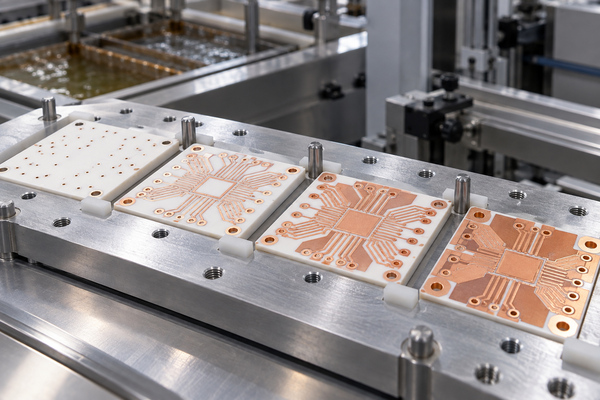
At BSTCeramicPCB, we review the finished circuit rather than only the artwork. The drawing and RFQ should therefore state finished dimensions, copper thickness, surface finish and acceptance methods, not just nominal design data.
What Should Prototype Inspection and Module Validation Cover?
Substrate inspection can cover outline, thickness, flatness, edge quality, registration, line/gap, pad dimensions, copper or finish thickness, via continuity, isolation and cleanliness. Representative cross-sections or adhesion tests can be added where the risk justifies them.
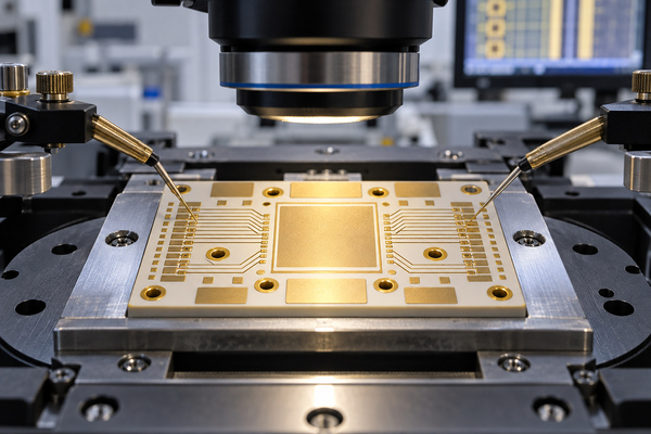
Module validation should then check detector noise, sensitivity, calibration stability, thermal drift, signal integrity and environmental reliability. These results belong to the completed assembly; they cannot be inferred from the substrate certificate alone.
What Information Should You Send Us in the RFQ?
Send us Gerber or ODB++ files, a dimensioned drawing, detector and readout footprints, ceramic material or performance requirements, thickness, copper thickness, finish, vias and critical tolerances. Add signal and grounding notes, heat sources, attach processes, temperature range, qualification requirements and quantities.
Email the package to sales@bstceramicpcb.com. We will review the ceramic route, conductor structure, panel method and inspection scope against the actual module inputs before quotation.
A DPC substrate for detector module integration is successful when thermal, electrical and mechanical decisions are connected. Treating it only as a small PCB leaves the detector's most important interfaces undefined.
 Products
 About us
 Contact us



