






















































 HOME
HOME

-

Ceramic PCB for Humanoid Robot joint actuators
2026 04,07 -
LTCC PCB Surprises: What Most People Miss
2025 12,09 -
Step-by-Step Guide to DPC PCB Design for Sensor Systems
2025 12,03 -
Ceramic PCBs Essential Benefits and Applications
2025 12,01 -
How Al2O3 DPC Ceramic Substrate PCB Enhances Heat Dissipation in Modern Electronics?
2025 11,28 -
How to Choose Between Ceramic, FR4, and Metal Core PCBs
2025 11,27 -
DPC Ceramic PCB Materials: Surprising Science Inside
2025 11,26 -
Wire bondable 2-layer Alumina substrates PCB | Bstceramic PCB
2025 09,22 -
Silicon Nitride Substrate, Silicon Nitride Ceramic Substrate Formula
2025 05,08 -
What is thick film ceramic PCB?
2023 08,02
Filled Vias Alumina Substrates: Design Rules and Applications
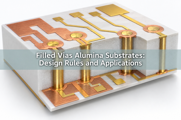
Filled vias alumina substrates combine an electrically insulating Al2O3 base with conductive vertical paths through the ceramic. They are used when a design needs a short ground connection, heat transfer through the substrate, two-sided routing, or a flat mounting surface above a via. The key decision is not simply whether a via can be filled, but which fill system, geometry, metallization, and inspection plan fit the circuit and assembly process.
What Are Filled Vias Alumina Substrates?
Filled vias alumina substrates are ceramic circuit bases with holes that pass through the alumina and are substantially occupied by conductive material. The fill creates a vertical electrical or thermal connection between the top and bottom metallization. The finished via may then be planarized so a trace, die-attach area, or pad can cross the opening.
The term is narrower than a generic ceramic PCB via. A plated through via has metal on the wall and an open center. A plugged hole may be closed mainly to control solder or contamination. A solid or paste-filled via is designed as a conductive column. Through alumina vias therefore need to be specified by function and process, not only by hole diameter.
How Does a Filled Via Work in Alumina?
Alumina provides dielectric isolation and mechanical support, while the metallic fill provides a low-resistance path through the thickness. The same column can serve three different purposes:
- connect a top conductor to a backside ground plane;
- move heat from a device attach area toward a carrier or heat spreader;
- route a signal between both sides of a ceramic circuit.
These functions are related but not interchangeable. A via optimized for RF grounding may be placed in an array close to a device. A thermal via must connect into a complete heat path. A signal via requires controlled transitions and pad geometry. The drawing should identify the intended function so the manufacturer can review the correct variables.
Filled Vias vs Plated Through Vias
The choice starts with the required electrical path, surface condition, assembly method, and cost. A filled structure offers the strongest case when the via must sit under a component or carry significant current or heat. A plated hole remains practical when an open bore does not interfere with assembly.
| Decision factor | Filled via | Plated through via |
|---|---|---|
| Conductive cross-section | Metal or conductive fill occupies most of the hole | Conductive layer follows the hole wall |
| Surface above the via | Can be planarized for via-in-pad or die attach | Opening normally remains visible |
| DC and RF resistance | Usually lower for the same finished geometry | Higher because current is limited to the plated wall |
| Thermal path | Stronger vertical conduction when connected to the heat spreader | Useful, but the open center limits metal area |
| Solder or adhesive control | Helps block bleed-through after proper planarization | Open holes may wick solder or adhesive |
| Process complexity | Higher; fill, cure or firing, and polishing must be controlled | Lower and more flexible for many designs |
| Typical reason to choose | RF grounding, thermal transfer, via-in-pad, two-sided dense circuits | General interconnection where an open hole is acceptable |
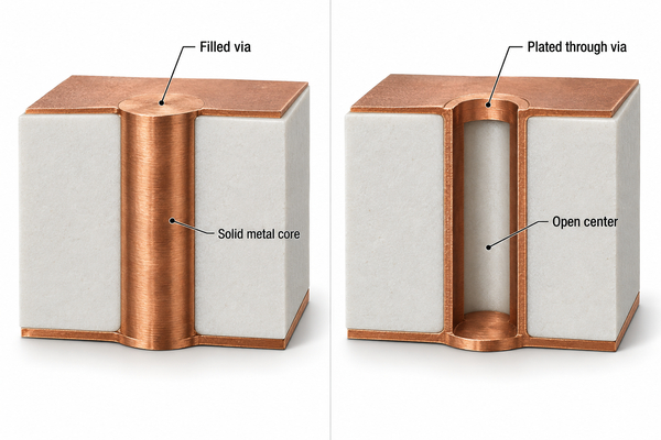
Filled vias are not automatically better. If a plated hole meets resistance, RF, thermal, and assembly requirements, specifying a fill adds process steps and cost without improving the product.
When Should You Specify Filled Vias?
Specify a conductive fill when at least one requirement cannot be met reliably with a plated opening. Strong use cases include a semiconductor die located over the via, a short ground path for an RF device, a concentrated heat source above a backside heat spreader, or a dense double-sided circuit where edge wrap consumes too much area.
A filled vias PCB design is usually unnecessary when the via only carries a low-current signal, the component can be placed away from the hole, surface planarity is not critical, and thermal analysis shows that the alumina and external heat sink already provide sufficient margin. This boundary should be decided before layout release because late conversion can change hole size, pad diameter, spacing, and the metallization flow.
Which Via Fill Materials Are Used?
The fill material must match the substrate, conductor system, firing or plating route, finish, and operating environment. The same word “filled” can describe very different processes.
| Fill route | Typical use | Main advantage | Main design caution |
|---|---|---|---|
| Solid copper | Thin-film or plated structures requiring low electrical and thermal resistance | High conductivity and lower material cost than gold | Copper expansion, oxidation control, adhesion, and planarization must be managed |
| Solid gold | High-reliability or specialized thin-film circuits | Stable surface and strong corrosion resistance | High material cost makes via volume important |
| Silver or copper conductive paste | Screen-printed or fired via filling | Compatible with scalable paste deposition | Shrinkage, porosity, firing atmosphere, and final resistivity depend on the paste system |
| Refractory co-fired metal | HTCC multilayer structures | Vias can be formed with internal conductors during ceramic firing | Conductor selection and shrinkage must match the co-fired ceramic system |
Requests for vias filled with copper should state whether solid copper, electroplated fill, or copper paste is intended. For multilayer ceramic packages, an HTCC ceramic substrate for satellite communication follows a different via formation route from a post-fired thin-film alumina circuit.
Substrate Thickness and Filled Via Geometry
The drilled depth is essentially the substrate thickness, so thickness directly affects the feasible via diameter and aspect ratio. A thicker plate with an overly small hole is harder to drill, coat, fill without trapped voids, and polish without recess or protrusion. A thinner plate allows smaller vias but becomes more sensitive to breakage and handling stress.
The manufacturer should review these related dimensions as one set:
- alumina thickness and thickness tolerance;
- drilled and finished via diameter;
- via aspect ratio;
- center-to-center pitch and edge clearance;
- capture-pad diameter and annular allowance;
- conductor clearance on both sides;
- finished surface recess or protrusion after polishing.
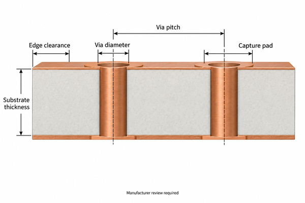
Do not copy a hole table from another process into a controlled drawing. Laser, ultrasonic, mechanical, paste-fill, electroplating, and co-fired processes have different windows. Provide the functional target and let the selected manufacturer confirm a buildable geometry.
RF, Grounding and Signal Integrity Considerations
At RF and microwave frequencies, a via behaves as a parasitic resistance and inductance rather than an ideal short. Filled vias can reduce resistive loss and provide a compact ground return, but performance still depends on via length, diameter, pad shape, number of vias, pitch, substrate dielectric properties, and the transition into the backside ground plane.
Place ground vias near the device connection they serve. Long lateral traces between the device and via reintroduce inductance. For via arrays, increasing quantity can reduce impedance only until crowding, ceramic strength, and manufacturing yield become limiting. Simulate the complete launch or grounding structure, then confirm that the proposed array respects drilling and edge-clearance rules.
A double-sided Al2O3 DPC ceramic circuit is a relevant product route when the application needs patterned metal on both sides and vertical connections, but the filled-via requirement must be reviewed separately from the surface DPC copper specification.
Thermal Design and Heat Flow
A metal-filled via can bypass part of the alumina thickness and create a vertical heat path, but it does not replace the rest of the thermal stack. The useful heat flow is limited by die attach, top pad spreading, via-to-pad interfaces, backside metallization, solder or braze, carrier, thermal interface material, and heat sink.
Use a compact thermal-resistance model or finite-element analysis when the heat source is small or power cycling is severe. Compare temperature with and without the via array, and verify current density if the same vias also carry electrical current. A dense array can improve through-thickness conduction while reducing the remaining ceramic ligament, so thermal benefit and mechanical robustness must be balanced.
Surface Planarity, Via-in-Pad and Assembly
Via-in-pad on ceramic is valuable when component footprint area is limited, but it makes surface finish a functional requirement. A recessed fill can trap solder or adhesive and tilt a die. A protruding fill can create a local stress point. Smear, dishing, exposed pores, or a weak interface can also reduce adhesion of the overlying metallization.
Specify the assembly method before defining planarity. Soldered components, silver sinter, conductive epoxy, eutectic die attach, and wire-bonded bare die do not have the same flatness or finish needs. Pad dimensions should account for the finished via and the overlying metal stack, not only the drilled hole.
Manufacturing Risks and Inspection
The most important defects are incomplete fill, internal voids or seams, cracks at the ceramic edge of the via, poor adhesion, excessive surface recess, and electrical discontinuity. Copper and alumina also expand differently during temperature changes, so large solid metal areas or aggressive thermal cycling can create interface stress.
Inspection should match the risk:
- optical inspection and profilometry for surface planarity;
- continuity and resistance measurements for electrical connection;
- X-ray or computed tomography for internal void screening where resolution permits;
- polished cross-sections for fill, wall condition, interfaces, and metallization thickness;
- thermal cycling, power cycling, or high-temperature storage for the intended environment;
- adhesion or shear testing for critical die-attach and pad structures.
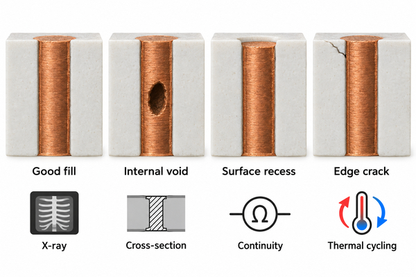
A prototype lot should define acceptance evidence before production. “No voids” is often not a practical inspection statement unless the drawing also defines the method, sampling plan, detectable size, and acceptance threshold.
Typical Applications
Filled vias alumina substrates are most useful where electrical, thermal, and packaging constraints overlap:
- RF and microwave modules requiring short ground returns;
- laser diode, photonics, and sensor submounts with localized heat sources;
- power modules and driver circuits with backside heat extraction;
- bare-die and hybrid circuits using via-in-pad or die-over-via layouts;
- compact two-sided ceramic circuits and hermetic package feedthrough structures;
- high-reliability aerospace, medical, automotive, and industrial electronics after application-specific qualification.
For sensor circuits, a 96% Al2O3 DPC ceramic substrate PCB illustrates an alumina circuit platform that can be evaluated for vertical interconnect requirements during DFM review.
Manufacturing Data Required for DFM Review
A useful DFM review requires more than a Gerber file. Send the following information together:
- alumina grade, purity, dimensions, and thickness;
- via function: ground, signal, thermal, or combined;
- hole diameter, position, pitch, edge distance, and quantity;
- preferred fill material and whether alternatives are acceptable;
- top and bottom metallization stack, conductor thickness, and surface finish;
- required planarity, recess, protrusion, and via-in-pad use;
- assembly method, maximum process temperature, and operating temperature range;
- current, voltage, RF frequency, power dissipation, and heat-sink arrangement;
- inspection, cross-section, resistance, thermal-cycle, and traceability requirements;
- prototype and production quantities, panel or individual-part delivery, and drawings in controlled revision.
At BSTCeramicPCB, we use these inputs to separate critical requirements from preferences and to identify conflicts before manufacturing release. Early review is especially important when the design combines small vias, thick alumina, dense arrays, large metal pads, or a strict planar surface.
FAQ
Should vias be filled in every alumina circuit?
No. Fill the via when an open plated hole cannot meet grounding, heat-transfer, via-in-pad, leakage-control, or mechanical requirements. Otherwise, a plated through via may be simpler and more economical.
Are filled vias and thermal vias the same?
Not always. A filled via becomes a useful thermal via only when its metal column connects the heat source to a lower-resistance path on the opposite side. Some filled vias are used mainly for signal or ground connections.
Can alumina vias be filled with resin?
Resin-filled vias are common terminology in organic PCB fabrication, but they are not equivalent to a conductive metal-filled ceramic via. If the goal is electrical or thermal conduction through alumina, specify a conductive fill system.
Can components be mounted directly over a filled via?
Yes, when the fill is fully processed and the surface meets the required planarity, metallization, and finish criteria. The assembly material and die size determine how strict those criteria must be.
What causes cracks around filled vias?
Common contributors include aggressive hole geometry, insufficient ceramic ligament, drilling damage, fill shrinkage, metal-to-ceramic expansion mismatch, polishing stress, and thermal cycling. Cross-section and reliability testing help separate manufacturing defects from design-driven stress.
How should manufacturing proposals be compared?
Compare the assumed alumina grade, fill route, via geometry, planarity, inspection, test coupons, yield basis, and included documentation. Two proposals are not equivalent if one includes verified planarization and cross-section testing while the other only includes basic continuity.
Filled vias can make an alumina circuit smaller, cooler, and easier to assemble, but only when the via is designed as part of the complete electrical, thermal, and manufacturing stack. For a review of filled vias alumina substrates, send your controlled drawings, material requirements, assembly conditions, and test expectations to sales@bstceramicpcb.com.
 Products
 About us
 Contact us



