






















































 HOME
HOME

-

Ceramic PCB for Humanoid Robot joint actuators
2026 04,07 -
LTCC PCB Surprises: What Most People Miss
2025 12,09 -
Step-by-Step Guide to DPC PCB Design for Sensor Systems
2025 12,03 -
Ceramic PCBs Essential Benefits and Applications
2025 12,01 -
How Al2O3 DPC Ceramic Substrate PCB Enhances Heat Dissipation in Modern Electronics?
2025 11,28 -
How to Choose Between Ceramic, FR4, and Metal Core PCBs
2025 11,27 -
DPC Ceramic PCB Materials: Surprising Science Inside
2025 11,26 -
Wire bondable 2-layer Alumina substrates PCB | Bstceramic PCB
2025 09,22 -
Silicon Nitride Substrate, Silicon Nitride Ceramic Substrate Formula
2025 05,08 -
What is thick film ceramic PCB?
2023 08,02
How Does Gold Wire Bonding Work on Ceramic PCBs?
Gold wire bonding connects semiconductor die pads to metallized circuit pads using fine gold wire. On a ceramic PCB, the wire bonds to a prepared metal surface, not to bare alumina or aluminum nitride. A reliable connection requires compatible pad metallurgy, a controlled bonding process and enough space for the wire loop and bonding tool.
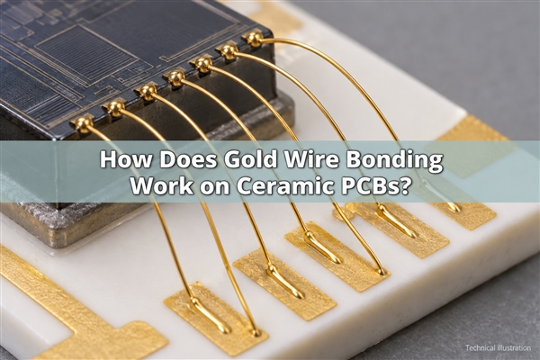
For ceramic circuit design, the first decision is whether the package needs a flexible chip-to-substrate interconnect or a shorter connection such as a flip-chip bump. Gold is ductile and resists oxidation, which helps produce consistent fine-wire connections. Its material cost and the electrical parasitics of a wire loop still need to be justified by the assembly.
How Does the Gold Wire Bonding Process Work?
The gold wire bonding process creates localized metal-to-metal joints through pressure and, in common thermosonic processes, heat and ultrasonic energy. It does not use solder paste or a reflow joint.
Die attach and wire bonding are separate operations. Die attach secures the chip and establishes its mechanical and thermal connection to the substrate. Wire bonding then connects the exposed die pads to the circuit. An unstable die, uncured adhesive or contamination from earlier assembly can prevent repeatable bonding even when the ceramic board dimensions are correct.
In gold ball wire bonding, the sequence is:
- An electronic flame-off discharge melts the wire tail to form a free-air ball below the capillary.
- The capillary presses that ball onto the first pad, usually on the die, to form a flattened ball bond.
- The tool rises and moves toward the second pad while paying out wire to form the loop.
- The capillary presses the wire onto the receiving pad to form a stitch bond, then the wire is terminated for the next cycle.
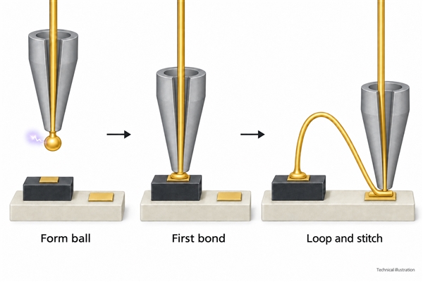
The discharge melts the free wire end; it does not mean that the die pad must melt. The bond interface is formed by deformation and solid-state joining under the selected process conditions.
How Is Gold Wire Bonding Temperature Selected?
Gold wire bonding temperature is a process variable, not a single material specification. The required setting changes with pad metallurgy, wire grade, tool design, ultrasonic input and the thermal limits of the die-attach material. The stage setpoint also does not necessarily equal the bond-interface temperature. A ceramic substrate's heat resistance alone does not establish a safe temperature for the complete assembly.
Start with the temperature limits of the assembled parts, including the die attach, nearby components and any existing polymer layers. Then establish whether heat is supplied through the workholder, the bonding tool or both. A process using a heated capillary can deliver heat differently from one relying on a heated stage, so transferring the stage setting between machines is not a reliable starting specification.
For a ceramic circuit, the substrate thickness, metallization and contact with the workholder affect how the assembly heats. Evaluate representative assemblies using the intended wire and pads, and compare joint strength and pad damage across the proposed settings. The useful result is a repeatable process window for that construction, not simply the highest temperature the ceramic can withstand.
Gold Ball Bonding vs Gold Wedge Bonding
Choose between these types of wire bonding by checking pad geometry, access direction, loop requirements and production throughput. Both can use gold, but their tools and bond footprints differ.
| Feature | Gold ball bonding | Gold wedge bonding |
|---|---|---|
| Typical first joint | Flattened ball | Elongated wedge bond |
| Typical second joint | Stitch bond | Wedge bond |
| Tool | Capillary with wire through its bore | Wedge tool with a directional wire feed |
| Layout consideration | Circular first-bond footprint and capillary clearance | Footprint length and tool approach direction |
| Common reason to select it | Fast, repeatable fine-wire chip interconnection | Directional access, low-loop designs or ribbon-compatible arrangements |
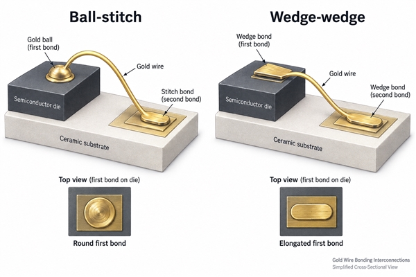
Gold ribbon wire bonding uses a flat conductor rather than round wire. It can be useful where a wider, lower-profile interconnect supports RF or current-carrying requirements, but it requires compatible tooling and a pad designed for the ribbon footprint.
Which Ceramic PCB Surfaces Support Gold Wire Bonding?
Bondability comes from the exposed metallization and its condition. The ceramic underneath provides insulation and mechanical support; changing from alumina to AlN does not automatically make the surface wire-bondable.
Our thin-film ceramic circuits for wireless communication include alumina constructions with gold-bearing metallization. For a bonded assembly, the top metal, underlying adhesion and barrier layers, pad flatness and cleaning history must be considered together. A gold-colored finish alone is not an adequate specification.
| Surface system | Bonding consideration | Important boundary |
|---|---|---|
| Thin-film or plated soft-gold pad | Specify the complete metal stack and usable bond area | Decorative or wear-resistant hard gold is not an interchangeable finish |
| Wire-bondable fired gold conductor | Paste formulation, firing and surface condition affect the joint | A generic thick-film conductor is not automatically suitable |
| ENEPIG over copper | Nickel-palladium-gold can support a qualified gold-wire process | Confirm deposit chemistry, layer control and assembly history |
| ENIG over copper | Suitability must be demonstrated for the specific wire and process | Solderability does not prove wire bondability |
| Aluminum die pad | Gold can form a bond to aluminum | Intermetallic growth and aging behavior need package-specific evaluation |
How Much Gold Thickness Is Needed for Wire Bonding?
There is no universal gold thickness for wire bonding across all these systems. An immersion-gold layer over palladium and a thicker soft-gold bonding layer have different functions and cannot be judged by the same thickness threshold. More gold does not repair poor adhesion, surface contamination or an unsuitable underlying layer.
Define the complete finish before choosing a thickness: the base conductor, adhesion or barrier layers, exposed bonding metal and deposition process. The specification should distinguish a nominal thickness from an acceptable thickness range at the bond pad. A board-wide average can obscure variation at a small bonding feature; measurement locations should represent the pads used in the assembly.
For soft-gold pads, purity and hardness belong alongside thickness in the surface specification. For ENEPIG, the nickel-palladium-gold stack must be assessed as a system. In either case, evaluate bondability after the thermal and handling steps that precede bonding, using representative finished circuits or coupons. This connects the coating specification to an actual joint instead of relying on appearance alone.
For example, our nickel-palladium-gold DBC ceramic PCB combines a copper circuit with a separate surface-finish system. DBC describes the copper-to-ceramic construction; it does not specify the gold-wire bonding recipe or guarantee the finished joint.
Gold wire bonding to copper also requires a defined surface condition. Do not treat bare copper and copper protected by a qualified bondable finish as equivalent: oxidation, storage and preparation change the interface.
What Wire Diameter and Pad Geometry Are Needed?
Gold wire bonding diameter must match the current, span, pad size and available tool. A 25 um wire is a common fine-wire example, not a universal requirement. One mil is exactly 25.4 um, so nominal metric and imperial descriptions should be checked against the wire specification rather than assumed identical.
Gold bonding wire is supplied in different purity and alloy grades. Two wires with the same nominal diameter can differ in elongation, breaking load, loop stability and free-air-ball behavior. These differences matter when the assembly has tight pad pitch or a low package lid.
Wire bonding pad design must provide room for the formed bond and tool, not just the wire diameter.
| Design feature | What must be controlled |
|---|---|
| Bond pad dimensions | Entire ball, stitch or wedge footprint plus placement allowance |
| Tool access | Clearance from the die edge, nearby components, cavity walls and adjacent wires |
| Loop height | A stated reference plane and clearance below the lid or encapsulation envelope |
| Bond span | Wire length, mechanical stability and electrical inductance |
| Pad spacing | Separation after bonding deformation and placement variation |
| Metallization attachment | Adhesion to the ceramic under bonding force and later thermal cycling |
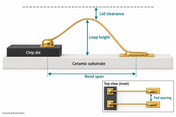
For RF circuits, the wire is part of the electrical design. Shortening a loop changes its inductance and coupling; adding parallel wires is not automatically equivalent to replacing one wire with a thicker conductor. Assess the actual loop geometry and return path at the operating frequency.
How Do Gold Wire Bonds Fail?
A gold wire bond can fail at the bonded interface, within the wire or beneath the pad. Identifying the failure location is more useful than treating every open circuit as insufficient bonding force.
| Observed problem | Possible cause | What to verify |
|---|---|---|
| Non-stick or lifted bond | Contamination, unsuitable surface or inadequate process energy | Surface condition and bondability before changing the recipe |
| Broken heel or neck | Excessive deformation, unsuitable loop or repeated strain | Tool condition, loop geometry and fracture location |
| Pad lift or cratering | Weak underlying layers or excessive mechanical stress | Metallization adhesion and die-pad support |
| Wire sweep or shorting | Wire movement during encapsulation or insufficient spacing | Completed package geometry, not only the open assembly |
| Degradation after aging | Metallurgical changes, corrosion or thermal stress | The actual metal pair, temperature exposure and package environment |
Gold wire bonding to aluminum is established technology, but the Au-Al interface changes with temperature and time. Initial electrical continuity alone does not establish long-term reliability. The die-pad metallurgy, wire grade and expected service exposure belong in the qualification plan.
How Are Gold Wire Bonds Tested?
Gold wire bonds are evaluated through inspection, electrical checks and mechanical tests that answer different questions. Electrical continuity confirms a conducting path; mechanical testing helps establish whether the wire and bonded interfaces withstand the specified loading. Initial bond strength and long-term package reliability are separate evaluations.
Wire pull and ball shear tests examine different aspects of the joint. Pull results depend on wire diameter, loop geometry and hook position; shear results depend on bond geometry and tool placement. Use an applicable acceptance method with defined conditions and record failure mode as well as force. A single force limit copied from a different wire size or package is not a defensible acceptance criterion.
For a ceramic circuit, distinguish a wire break from a lifted metal pad or a separation within the finish. These outcomes point to different parts of the interconnect: wire properties and loop geometry, metallization attachment, or the bonding interface. A force result without the fracture location leaves that distinction unresolved.
Where the package must withstand temperature cycling or prolonged high-temperature exposure, qualification should examine the completed construction after the relevant stress sequence. Die attach, encapsulation and the lid can affect the wires even when the bare ceramic remains stable. Destructive tests require designated samples; their results should not be confused with a claim that every shipped bond was pull-tested.
Gold vs Aluminum Wire Bonding: When Is Each Suitable?
Gold vs aluminum wire bonding is a choice of material, process and package architecture, not simply which metal conducts better. Compare the complete interconnect and its qualification requirements.
| Option | Where it can fit | Main trade-off |
|---|---|---|
| Fine gold wire | Compact signal connections and established thermosonic processes | Material cost and compatibility of the bonded metal pair |
| Aluminum wire | Ultrasonic wedge bonding and many power-module interconnects | Different oxide behavior, tooling and bond geometry |
| Copper wire | Assemblies that can support a qualified lower-cost wire system | Oxidation control and mechanical loading on sensitive pads |
| Flip-chip connection | Designs needing short interconnects or area-array connections | Bumping, alignment and package stress management |
Heavy wire bonding in a power module should not be replaced by fine gold wires solely because the substrate is ceramic. Current distribution, wire count, thermal cycling and available pad area may favor aluminum, copper, ribbon or another package connection.
Gold wire bonding price is driven by more than the gold content. Bond count, wire dimensions, loop complexity, setup and qualification all affect assembly cost. A change that reduces wire cost but requires a new pad finish or a different package process may not reduce the total manufacturing cost.
Where Does Gold Wire Bonding Fit in Ceramic Assemblies?
Gold wire bonding fits ceramic assemblies when exposed die pads need short, controlled connections to a stable metallized substrate. The relevant use cases differ in what the circuit must preserve:
- RF and microwave modules need repeatable wire geometry, ground connections and clearance around matching structures.
- Photonic assemblies need electrical connections that do not obstruct optical paths or interfere with die alignment and package closure.
- Sensor and medical-electronics hybrids need stable small-signal connections and a bonding process compatible with the surrounding components.
Our thin-film ceramic boards for medical electronics include 96% alumina constructions. For these circuits, selecting the substrate and metallization together allows the bond pads to be integrated into the layout. The board application does not by itself qualify the complete device or its wire bonds.
At BSTCeramicPCB, we provide thin-film and other ceramic circuit constructions for integration into these assemblies. For Gold wire bonding, the decisive checks are the exposed pad metal, bond footprint, wire-loop envelope and qualified assembly process. Contact sales@bstceramicpcb.com to discuss a ceramic circuit and metallization suitable for your package design.
 Products
 About us
 Contact us



