






















































 HOME
HOME

-

Ceramic PCB for Humanoid Robot joint actuators
2026 04,07 -
LTCC PCB Surprises: What Most People Miss
2025 12,09 -
Step-by-Step Guide to DPC PCB Design for Sensor Systems
2025 12,03 -
Ceramic PCBs Essential Benefits and Applications
2025 12,01 -
How Al2O3 DPC Ceramic Substrate PCB Enhances Heat Dissipation in Modern Electronics?
2025 11,28 -
How to Choose Between Ceramic, FR4, and Metal Core PCBs
2025 11,27 -
DPC Ceramic PCB Materials: Surprising Science Inside
2025 11,26 -
Wire bondable 2-layer Alumina substrates PCB | Bstceramic PCB
2025 09,22 -
Silicon Nitride Substrate, Silicon Nitride Ceramic Substrate Formula
2025 05,08 -
What is thick film ceramic PCB?
2023 08,02
How to Choose a High Thermal Conductivity PCB for Power Electronics?
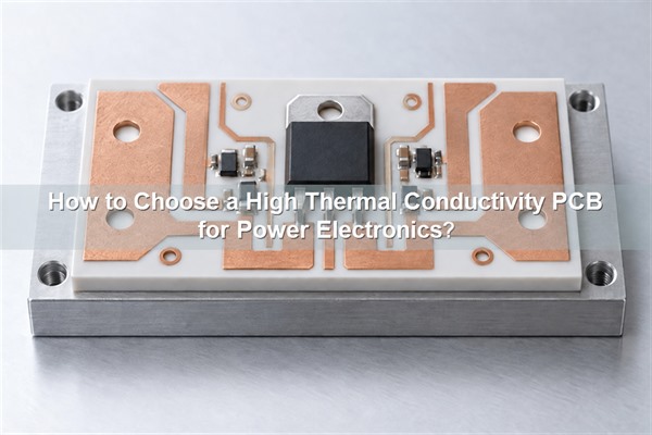
A High thermal conductivity PCB moves heat from power components to a heat spreader, housing, cold plate, or ambient environment without exceeding the allowed junction temperature. The right board is not simply the material with the largest W/m·K value. Selection must consider dielectric thickness, copper coverage, interfaces, electrical isolation, thermal cycling, mechanical load, circuit density, and cost.
What Is a High Thermal Conductivity PCB?
A high thermal conductivity PCB is a circuit board designed with a substrate, dielectric, copper structure, and assembly stack that carry heat more effectively than conventional FR4. The term can describe thermally enhanced laminates, metal-core PCBs, copper-base PCBs, or ceramic PCBs. These constructions do not provide the same heat path or electrical performance.
For power electronics, the useful specification is the thermal resistance from the device junction or case to the cooling surface. Bulk material conductivity is one input to that resistance, not the final answer.
Why Is Thermal Conductivity Alone Not Enough?
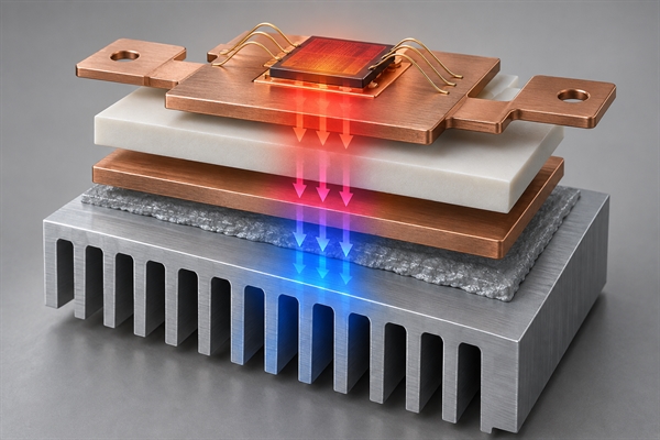
Thermal conductivity describes how readily heat passes through a material. PCB temperature rise depends on the complete path: component attach, copper, dielectric or ceramic, metallization interfaces, thermal interface material, and heat sink. A thin 2 W/m·K dielectric can produce lower through-thickness resistance than a much thicker material with a higher conductivity.
The published value must also identify direction and test conditions. Laminates can conduct heat differently through the thickness and in the plane, while copper planes and thermal vias make the assembled PCB highly anisotropic. Compare supplier data at the same temperature and in the same direction.
Which PCB Materials Offer High Thermal Conductivity?
Use conductivity ranges for initial screening only. Final calculations should use the selected grade's datasheet value and tolerance.
| High thermal conductivity PCB material | Typical conductivity range | Electrical isolation | Main selection point |
|---|---|---|---|
| Standard FR4 | About 0.3-0.6 W/m·K | Yes | Low cost and multilayer routing, but limited through-thickness heat flow |
| Thermally enhanced laminate | About 1-3 W/m·K; some specialty grades are higher | Yes | Preserves familiar PCB processing for moderate heat loads |
| Metal-core dielectric | Commonly about 1-10 W/m·K for the dielectric layer | Yes | Thin dielectric over aluminum or copper gives a short path to a metal spreader |
| Alumina ceramic | Commonly about 20-30 W/m·K | Yes | Cost-effective ceramic insulation and stable high-temperature behavior |
| Aluminum nitride ceramic | Commonly about 140-180 W/m·K | Yes | High heat flow with a CTE closer to semiconductor materials than metals |
| Silicon nitride ceramic | Grade-dependent, often below AlN | Yes | High fracture toughness and strong thermal-cycle reliability |
| Copper | About 390-400 W/m·K | No | Excellent spreading and current capacity, but requires an insulating layer where isolation is needed |
A high thermal conductivity aluminum PCB may be marketed using the conductivity of the metal core rather than the insulating dielectric. For device-to-baseplate heat flow, the thin dielectric layer often controls the result, so compare its thickness, conductivity, and isolation rating instead of relying on the aluminum value alone.
Ceramic PCB vs MCPCB vs FR4
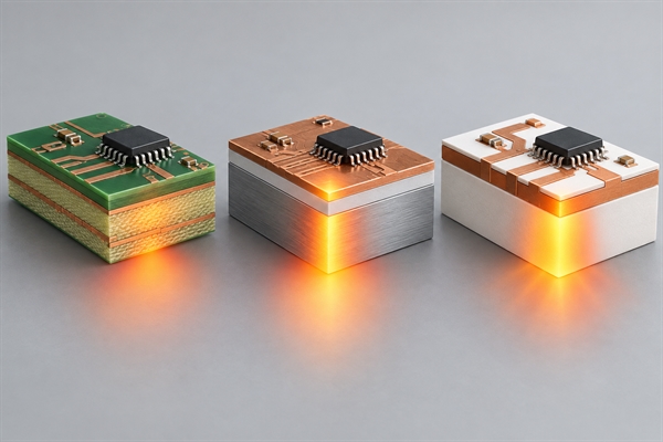
Choose the construction by heat flux, isolation voltage, routing complexity, mechanical conditions, and production cost rather than by a single material property.
| Construction | Best fit | Main limitation | Buyer decision |
|---|---|---|---|
| FR4 or thermally enhanced laminate | Multilayer logic, control, and moderate power density | Low through-thickness conductivity; thermal vias consume routing area | Use when copper planes, vias, and external cooling keep temperatures within limits |
| Aluminum MCPCB | LEDs, converters, and single-sided power circuits with a direct baseplate path | The dielectric limits thermal and electrical performance; multilayer options are constrained | Use when cost and metal spreading matter more than ceramic stability |
| Copper-base PCB | Very high local heat flux and current | Weight, cost, and dielectric-interface constraints | Use when maximum spreading is required and the mechanical penalty is acceptable |
| Ceramic PCB | High isolation, high temperature, compact power density, RF, and matched expansion needs | Brittle handling and higher process cost | Use when organic dielectric or metal-core interfaces are the reliability limit |
FR4 remains the practical choice when the calculated thermal margin is adequate. A ceramic upgrade is justified by measurable temperature, isolation, size, or reliability requirements, not by the desire to specify the highest conductivity.
How Do You Choose Between Alumina, AlN, and Silicon Nitride?
Ceramic grades solve different problems. Conductivity, toughness, copper attachment, CTE, substrate thickness, and lifetime targets must be reviewed together.
| Ceramic substrate | Why buyers choose it | When it may be unnecessary | Critical review item |
|---|---|---|---|
| Alumina (Al2O3) | Balanced cost, insulation, chemical stability, and established thick-film/DPC/DBC processing | When heat flux requires a much lower substrate resistance | Verify purity, conductivity grade, thickness, and flatness |
| Aluminum nitride (AlN) | Highest commonly used ceramic-substrate conductivity and favorable expansion for semiconductor devices | When alumina already meets the temperature target | Control moisture handling, metallization compatibility, and grade-specific conductivity |
| Silicon nitride (Si3N4) | High fracture toughness and strong resistance to power cycling | When peak conductivity is more important than mechanical reliability | Review AMB/metal-bond system, strength data, and thermal-cycle requirement |
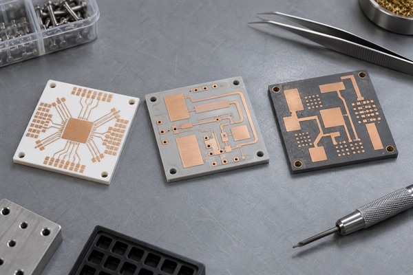
For concentrated LED or laser heat, an AlN DPC ceramic PCB can shorten the path from the device to the heat spreader. An alumina DPC ceramic circuit board is often sufficient when cost matters and the calculated substrate drop is acceptable. For traction inverters and repeated power cycling, a silicon nitride AMB ceramic substrate may offer a better mechanical-reliability trade-off.
Is High-Tg PCB the Same as a High Thermal Conductivity PCB?
No. Glass transition temperature, or Tg, indicates where a polymer laminate changes mechanical behavior. Thermal conductivity indicates heat-transfer capability. A high-Tg laminate can tolerate a higher processing or operating temperature without having a high through-thickness conductivity.
High temperature PCBs may need high Tg, low Z-axis expansion, thermal stability, and low thermal resistance, but those are separate specifications. Do not substitute Tg for W/m·K in a thermal model.
How Do You Estimate Thermal Resistance Through the Stack-Up?
For a uniform layer, a first-pass through-thickness estimate is:
Rth = t / (k × A)
where t is layer thickness in meters, k is thermal conductivity in W/m·K, and A is the effective heat-transfer area in square meters. Real assemblies also include spreading resistance and interface resistance, so this is not a complete PCB thermal conductivity calculator.
For example, doubling ceramic thickness doubles that layer's ideal one-dimensional thermal resistance. Increasing the effective copper spreading area reduces heat flux before it enters the substrate. Solder voids, die attach, surface flatness, thermal grease, clamping pressure, and baseplate contact can dominate even when the ceramic has a high conductivity.
How Do Copper Thickness and Layout Affect Heat Flow?
Copper spreads heat laterally and reduces current density. Heavy copper around a power device can lower local temperature, but copper that stops near the heat source or narrows abruptly can create a hot spot. Thermal vias can connect surface copper to internal or backside planes in laminate PCBs; their benefit depends on hole diameter, plating thickness, pitch, fill, and connection to a real heat-spreading surface.
A high thermal conductivity pad should be large enough to spread heat without violating creepage, clearance, solder control, RF impedance, or component-placement limits. On ceramic PCBs, copper thickess and pattern balance also affect stress, bow, and thermal cycling. The thermal design and manufacturability review should use the same copper artwork.
When Should You Choose a Ceramic Substrate?
Choose a high thermal conductivity PCB substrate based on a ceramic when one or more of these conditions apply:
- The device heat flux is too high for an organic dielectric at the available footprint.
- High voltage isolation must coexist with a short thermal path.
- The module experiences wide temperature swings or repeated power cycling.
- CTE mismatch between a metal base and a semiconductor threatens die attach or solder joints.
- RF loss, dimensional stability, hermetic packaging, or high operating temperature rules out FR4.
- The design needs DPC, DBC, AMB, thick-film, thin-film, or ceramic package features.
Ceramic is unnecessary when an FR4 thermal-via array or MCPCB meets junction-temperature and reliability limits with adequate margin. A prototype comparison can be more economical than over-specifying AlN for every design.
Common Applications in Power Electronics
High thermal conductivity substrates are used where a small area must carry significant heat and current while maintaining electrical isolation. Common applications include high-power LED modules, laser diode submounts, RF power amplifiers, IGBT modules, SiC and GaN converters, automotive inverters, DC-DC power stages, medical power devices, aerospace electronics, and industrial motor drives.
The same application can require different materials. A lighting board may use aluminum MCPCB, an isolated laser submount may use AlN DPC, and a traction module may use Si3N4 AMB. Device loss, duty cycle, cooling method, isolation voltage, and lifetime determine the appropriate platform.
Design and Manufacturing Limits
Ceramic PCB manufacturing limits depend on the process. Thick film supports economical printed conductors; DPC supports finer features and plated copper; DBC and AMB support thick bonded copper for power modules; thin film supports precision RF and microelectronic patterns. Line width, spacing, copper thickness, via type, metallization, surface finish, and panel handling limits are therefore process-specific.
Avoid specifying every tolerance at the tightest possible value. Excessively tight outline, thickness, flatness, hole, and pattern tolerances reduce yield without necessarily improving thermal performance. Control the dimensions that affect die placement, interface contact, registration, isolation, or assembly, and allow practical tolerance elsewhere.
For asymmetric copper, large solid areas, thin ceramics, or closely spaced edge features, review bow, stress concentration, singulation method, and fixture support before releasing the design.
Reliability and Validation Tests
Validate the complete assembly, not only a substrate coupon. The test plan should reflect actual power cycles, cooling, mounting force, interfaces, and environment.
| Validation item | What it confirms | Typical failure detected |
|---|---|---|
| Thermal impedance or structure-function test | Actual junction-to-case or case-to-sink path | Unexpected interface or spreading resistance |
| Infrared imaging or calibrated thermocouples | Hot-spot location and temperature distribution | Layout bottlenecks and uneven contact |
| Dielectric withstand and insulation resistance | Electrical isolation margin | Thin dielectric, contamination, or edge-clearance weakness |
| Thermal cycling and power cycling | CTE compatibility and fatigue life | Copper delamination, ceramic cracks, solder or die-attach fatigue |
| Metallization adhesion or peel testing | Copper-to-ceramic integrity | Weak bonding or process variation |
| Flatness, X-ray, and cross-section inspection | Assembly contact and internal quality | Bow, voiding, cracks, and interface defects |
Define acceptance limits before testing. A board that reaches a low temperature in an open-bench test may still fail after enclosure heating, mounting stress, or thousands of power cycles.
What Should You Provide for a Quote?
Provide the thermal and manufacturing requirements that control the design:
- Application, device type, continuous and peak power loss, duty cycle, and allowable junction or case temperature.
- Ambient or coolant temperature, heat-sink interface, airflow, mounting pressure, and available cooling area.
- Required substrate material and grade, or permission for the manufacturer to compare options.
- Ceramic or dielectric thickness, board dimensions, copper thickness, layer structure, circuit files, and drawing.
- Isolation voltage, creepage and clearance, surface finish, soldering or wire-bonding requirements.
- Flatness, dimensional tolerances, via or hole requirements, edge condition, and singulation method.
- Thermal, electrical, mechanical, and environmental test requirements.
- Prototype quantity, production forecast, target cost, and required delivery schedule.
At BSTCeramicPCB, we can review the material, copper structure, geometry, process route, and test inputs before quotation. Supplying the heat-source map and cooling boundary conditions prevents a high conductivity value from being treated as a substitute for a complete thermal design.
FAQ
What are common high-thermal-conductivity PCB materials?
Common choices include thermally enanced laminates, aluminum or copper metal-core boards, alumina, aluminum nitride, and silicon nitride ceramic substrates. The best material depends on heat flux, insulation, mechanical reliability, layout, and cost.
Is 8.5 W/m·K good for a PCB?
It is high for many polymer dielectric layers and may be suitable for an MCPCB, but it is lower than common ceramic-substrate values. Check whether 8.5 W/m·K describes the dielectric, bulk metal, or complete test structure, then calculate the actual layer resistance.
What material has the highest thermal conductivity in a PCB?
Copper has higher bulk conductivity than common PCB ceramics, but it is electrically conductive. Among electrically insulating ceramic PCB materials, AlN is usually selected when very high conductivity is required. The complete stack may still be limited by attach layers and interfaces.
Does a thicker ceramic substrate improve heat spreading?
It may spread heat laterally, but it also increases through-thickness resistance. Select thickness from mechanical strength, dielectric requirement, copper stress, handling, and the modeled thermal path rather than assuming thicker is cooler.
Can ceramic PCB replace a heat sink?
Usually not. Ceramic conducts heat from the device and can spread it, but the energy still needs to reach a baseplate, heat sink, cold plate, chassis, or airflow path.
Conclusion
The best High thermal conductivity PCB is the construction that meets junction-temperature, isolation, layout, mechanical, reliability, and cost targets with verified margin. Compare thermal resistance across the complete stack, then select FR4, metal-core, alumina, AlN, or Si3N4 from the actual heat path and service conditions. For a ceramic PCB material review or quotation, contact BSTCeramicPCB at sales@bstceramicpcb.com.
 Products
 About us
 Contact us



