






















































 HOME
HOME

-

Ceramic PCB for Humanoid Robot joint actuators
2026 04,07 -
LTCC PCB Surprises: What Most People Miss
2025 12,09 -
Step-by-Step Guide to DPC PCB Design for Sensor Systems
2025 12,03 -
Ceramic PCBs Essential Benefits and Applications
2025 12,01 -
How Al2O3 DPC Ceramic Substrate PCB Enhances Heat Dissipation in Modern Electronics?
2025 11,28 -
How to Choose Between Ceramic, FR4, and Metal Core PCBs
2025 11,27 -
DPC Ceramic PCB Materials: Surprising Science Inside
2025 11,26 -
Wire bondable 2-layer Alumina substrates PCB | Bstceramic PCB
2025 09,22 -
Silicon Nitride Substrate, Silicon Nitride Ceramic Substrate Formula
2025 05,08 -
What is thick film ceramic PCB?
2023 08,02
How to Design a High Voltage Ceramic PCB for Reliable Insulation
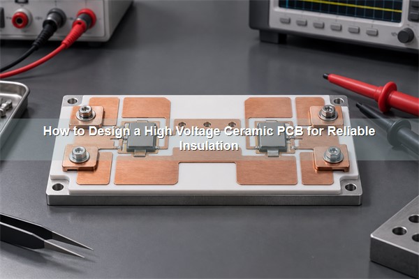
A high voltage ceramic PCB combines an electrically insulating ceramic substrate with patterned metal conductors for circuits that must control voltage stress, heat and mechanical stability in a compact assembly. Ceramic can provide a stronger insulation foundation than an organic laminate, but the finished board is not rated by ceramic dielectric strength alone. Working voltage depends on substrate thickness, conductor spacing, copper-edge geometry, contamination, altitude, coating or potting, transients and the test standard applied to the complete assembly.
What Is a High Voltage Ceramic PCB?
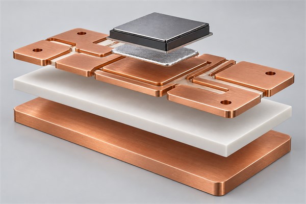
A high voltage ceramic PCB is a metallized alumina, aluminum nitride (AlN) or silicon nitride (Si3N4) substrate designed so conductive features remain electrically isolated at the specified continuous voltage, transient voltage and environmental condition. Depending on the current and thermal load, the circuit may use thin plated conductors, thick-film conductors, direct bonded copper (DBC) or active metal brazed (AMB) copper.
“High voltage” has no useful universal threshold for PCB layout. A voltage that is routine inside one controlled, encapsulated module may require wider spacing in exposed equipment at altitude or under pollution. The design must therefore begin with the applicable product standard, insulation category, waveform, overvoltage condition and environment rather than a generic voltage label.
Why Does Ceramic Help Without Defining the Voltage Rating?
Ceramic is a strong bulk insulator, resists heat and does not soften like an organic resin system. Its low moisture uptake and dimensional stability can help maintain conductor geometry through temperature changes. These properties are useful in compact power modules, but they address only part of the insulation system.
Three paths must be checked separately. Through-thickness voltage stresses the ceramic bulk between conductors on opposite faces. Clearance is the shortest path through air between conductive parts. Creepage is the shortest path along the ceramic or coating surface. A board can have adequate ceramic thickness and still flash over along a contaminated surface or across a narrow air gap.
Material dielectric-strength data also require context. Values vary with ceramic grade, specimen thickness, temperature, frequency, electrode geometry and test method. Use the controlled datasheet for the selected grade, then qualify the fabricated circuit and assembled module under the intended conditions. A catalog material value is not a safe substitute for a system working-voltage rating.
Which Ceramic Substrate Material Should You Choose?
Select the ceramic from electrical insulation, thermal resistance, mechanical loading and process compatibility together. Thermal conductivity is often the clearest material difference, but a higher value is only useful when heat actually crosses the ceramic layer.
| Material | Representative thermal conductivity at 20 C | High-voltage design value | Main trade-off |
|---|---|---|---|
| Al2O3 alumina | About 24 W/mK for a representative substrate grade | Mature insulating ceramic for cost-sensitive power and control circuits | Higher thermal resistance than AlN or Si3N4 when heat flux is concentrated |
| AlN | About 170 W/mK for a representative grade | High heat transfer with electrical isolation for dense power devices | Grade, moisture handling, metallization compatibility and cost need control |
| Si3N4 | About 90 to 110 W/mK for representative substrate grades | High fracture toughness and thermal-cycle durability for mechanically demanding modules | Higher material and process cost may be unnecessary for moderate cycling |
These are comparison values, not guaranteed specifications for every substrate. An Al2O3 ceramic PCB for high voltage applications can be the practical choice when heat flux and cycling are moderate. AlN is more useful when the ceramic layer limits junction-to-coolant resistance. Si3N4 becomes attractive when large copper areas, power cycling or mechanical loads make fracture resistance a primary risk.
How Do Creepage and Clearance Control Surface Flashover?
Clearance must withstand the electric field through air, including transient overvoltage and altitude effects. Creepage must resist tracking along a surface exposed to humidity, ionic residue, dust or condensation. The required distances depend on the applicable safety or insulation-coordination standard, working and impulse voltage, material group, pollution degree, altitude and whether insulation is basic, supplementary or reinforced.
Do not use one spacing number for every net pair. Classify each high-voltage boundary and identify the maximum potential difference under normal operation, startup, shutdown and fault. Then apply the correct requirement to conductor-to-conductor, conductor-to-heatsink, primary-to-secondary and board-to-enclosure paths.
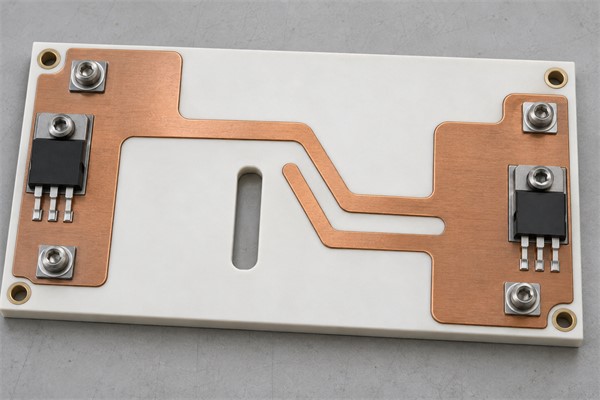
A slot can extend the surface path when it fully interrupts the relevant creepage route and is manufacturable without creating fragile ceramic webs. Coating or potting may reduce contamination exposure, but the material, thickness, void control, adhesion and qualification method must match the standard. Encapsulation should not be used to hide an uncontrolled air gap or a sharp copper edge.
How Should Copper Geometry and Board Edges Be Designed?
Electric fields concentrate at sharp conductor corners, narrow necks and copper edges near another potential. Use smooth radii where space permits, keep high-field copper away from the ceramic edge, and avoid opposing conductor edges that create a short direct path. The finished copper profile matters: etched sidewalls, plating buildup, burrs and metal residues can change the local field from the ideal CAD geometry.
Heavy copper adds current capacity and heat spreading but also increases etch undercut, step height and thermomechanical stress. Large asymmetric copper areas can bow a thin substrate or load the ceramic during thermal cycling. Copper thickness, pattern balance, ceramic thickness, minimum web width, edge setback and corner radius should be reviewed as one stack rather than independent drawing notes.
Keep mounting hardware and conductive baseplates inside the insulation model. A screw, clamp or heatsink can become the nearest grounded object even when it is absent from the ceramic artwork. Define the assembled distance to those parts and control conductive adhesive squeeze-out, solder overflow and wire-bond loop position.
Which Metallization Process Fits a High Voltage Ceramic PCB?
The process must support the required copper thickness, feature size, current, attachment method and thermal-cycle life. No process automatically delivers a higher voltage rating; voltage performance still depends on geometry, cleanliness, interfaces and qualification.
| Process | Best fit | High-voltage design check |
|---|---|---|
| DPC | Fine features, plated vias, compact routing and moderate copper thickness | Confirm finished spacing after plating and keep residues out of narrow isolation gaps |
| DBC | High current, strong lateral heat spreading and thick copper power layouts | Review etched copper edges, ceramic margin, copper balance and thermal stress |
| AMB | Power modules requiring robust metal-to-ceramic attachment, often with Si3N4 | Control braze-system geometry, exposed conductive residues and qualification after cycling |
| Thick film | Printed conductors, resistors and moderate-power functional circuits | Validate paste system, fired surface, conductor edge quality and environmental leakage |
For high-current switching modules, a DBC ceramic substrate for IGBT power devices is a relevant thick-copper construction. An AMB ceramic PCB for IGBT modules is more appropriate when the design also prioritizes mechanical robustness and power cycling. Fine routing or plated interconnect features can favor an AlN DPC ceramic substrate for power conversion.
What Tests Verify High Voltage Reliability?
Verification should reproduce the relevant voltage stress and environment instead of relying on a single room-temperature hipot result. Define test voltage, waveform, ramp, dwell, trip current, electrode connection, temperature and humidity before testing. A destructive margin test and a production screening test serve different purposes and should not be confused.
| Test | What it reveals | Important condition |
|---|---|---|
| Dielectric withstand or hipot | Gross insulation breakdown or excessive leakage at a defined stress | Specify AC/DC waveform, ramp, dwell, current limit and connected nodes |
| Insulation resistance | Surface or bulk leakage below breakdown | Measure at defined voltage, temperature, humidity and stabilization time |
| Partial-discharge test | Localized discharge in voids, interfaces or high-field regions before full breakdown | Define inception/extinction criteria, noise floor and assembly state |
| Thermal or power cycling | Cracks, delamination and interface degradation caused by CTE mismatch | Repeat electrical tests after cycling, not only before exposure |
| Humidity and contamination exposure | Loss of surface insulation and tracking margin | Use the expected coating, cleaning state and operating bias where applicable |
| Visual, cross-section or acoustic inspection | Edge defects, cracks, voids or interface separation | Choose inspection based on DPC, DBC, AMB or assembled-module construction |
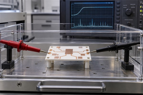
Partial-discharge performance is especially important when insulation must survive repeated high electric-field stress. A board can pass a brief withstand test yet develop discharge at a lower repetitive operating condition because of a void, edge field or contaminated interface. Test the representative mounted and encapsulated state whenever those interfaces alter the field distribution.
Where Are High Voltage Ceramic PCBs Used?
- EV traction inverters and onboard power conversion: DBC or AMB substrates combine isolation with high current and a short thermal path beneath IGBT, MOSFET or SiC devices.
- Industrial motor drives and servo power modules: ceramic supports repeated switching, elevated temperature and controlled isolation between power stages and grounded cooling hardware.
- Solar, energy-storage and UPS converters: high-voltage DC links require coordinated conductor spacing, surge withstand and heat removal. A double-sided DBC ceramic board for automotive power electronics illustrates a construction used where both thermal and electrical interfaces must be managed.
- High-voltage power supplies and pulsed electronics: waveform, repetition rate, edge field and partial discharge can matter more than nominal DC voltage alone.
- Medical and scientific equipment: compact high-voltage generation may use ceramic where stable insulation and low outgassing are required, but product-specific safety and leakage-current rules still govern the assembly.
Ceramic is unnecessary when FR4 or another qualified laminate already meets voltage, temperature, lifetime and size targets. A metal-core PCB can be economical for one-sided heat spreading, but its thin dielectric layer and grounded metal base create a different insulation problem. Choose ceramic when the combination of electrical isolation, temperature capability, dimensional stability, thermal path or package size justifies the material and process cost.
What Should Be Defined Before Fabrication?
The fabrication package must describe the electrical stress and assembled interfaces, not only the ceramic artwork. At minimum, define:
- continuous working voltage, maximum transient or impulse voltage, waveform, frequency, polarity and switching repetition;
- insulation function and applicable product or insulation-coordination standard;
- operating altitude, pollution exposure, humidity, temperature range and expected lifetime;
- ceramic material, controlled grade, finished thickness, flatness, edge condition and critical mechanical tolerances;
- metallization process, finished copper thickness, minimum spacing, edge setback, slots, vias and surface finish;
- baseplate, heat sink, fasteners, wire bonds, terminals, coating or potting that affect clearance and creepage;
- current and loss map, device locations, thermal interface and allowable junction or case temperature;
- prototype and production tests, including test voltage, duration, leakage limit, partial-discharge criterion and environmental preconditioning.
At BSTCeramicPCB, we can review the ceramic circuit portion against the specified material, copper structure, dimensions, isolation geometry, surface finish and test requirements. Final working-voltage approval remains tied to the complete assembly, its environment and the applicable standard, so those conditions should be shared before the layout and process are frozen.
FAQ
How many volts can a ceramic PCB handle?
There is no universal voltage value. The limit depends on ceramic grade and thickness, clearance, creepage, copper geometry, environment, transients, coating or potting and the qualified test method. Use the applicable standard and validate the completed assembly.
What is considered high voltage on a PCB?
The boundary depends on product category, safety standard and operating environment. Treat any circuit requiring dedicated insulation coordination, controlled spacing, surge evaluation or high-voltage testing as a high-voltage design problem rather than relying on one informal threshold.
What is the best PCB material for high-voltage applications?
No material is best by itself. Alumina, AlN and Si3N4 can all support high-voltage ceramic circuits when their grade, thickness, geometry and metallization are appropriate. Organic laminates may also be suitable when their certified material system and spacing meet the required voltage and environment.
Is a ceramic PCB better than FR4 for high voltage?
Ceramic offers higher temperature capability, low moisture uptake and stable bulk insulation, but it is more brittle and costly. FR4 can be the better choice when approved laminate ratings, spacing and thermal performance already meet the requirement.
Is an MCPCB the same as a high voltage ceramic PCB?
No. An MCPCB usually uses a metal base under a thin dielectric layer, while a ceramic PCB uses the ceramic itself as the insulating structural substrate. Both can spread heat, but their insulation paths, mechanical construction and qualification are different.
Does higher ceramic thermal conductivity improve voltage capability?
Not directly. Higher thermal conductivity can reduce temperature and therefore lower thermal stress, but voltage capability still depends on dielectric properties, geometry, environment, interfaces and testing.
Why test partial discharge if the board passes hipot?
Hipot checks for breakdown or excessive leakage at a defined stress. Partial-discharge testing can identify localized discharge in voids or high-field interfaces before complete breakdown, which matters under repetitive long-life operation.
Conclusion
A reliable high voltage ceramic PCB starts with the complete insulation system, not a ceramic dielectric-strength number. Select the material and metallization for the electrical, thermal and mechanical load; calculate bulk, clearance and creepage paths separately; reduce local field concentration; and verify the representative assembly after environmental and thermal stress. For a ceramic substrate design and manufacturing review, contact BSTCeramicPCB at sales@bstceramicpcb.com.
 Products
 About us
 Contact us



