






















































 HOME
HOME


-

Ceramic PCB for Humanoid Robot joint actuators
2026 04,07 -
LTCC PCB Surprises: What Most People Miss
2025 12,09 -
Step-by-Step Guide to DPC PCB Design for Sensor Systems
2025 12,03 -
Ceramic PCBs Essential Benefits and Applications
2025 12,01 -
How Al2O3 DPC Ceramic Substrate PCB Enhances Heat Dissipation in Modern Electronics?
2025 11,28 -
How to Choose Between Ceramic, FR4, and Metal Core PCBs
2025 11,27 -
DPC Ceramic PCB Materials: Surprising Science Inside
2025 11,26 -
Wire bondable 2-layer Alumina substrates PCB | Bstceramic PCB
2025 09,22 -
Silicon Nitride Substrate, Silicon Nitride Ceramic Substrate Formula
2025 05,08 -
What is thick film ceramic PCB?
2023 08,02
How to Select Ceramic PCB Metallization: DBC, DPC, AMB, Thick Film and Thin Film
Published:
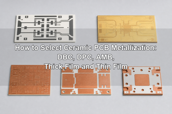
How to Select Ceramic PCB Metallization starts with the conductor requirement, not the ceramic name. Define the current, allowable temperature rise, minimum line and gap, bonding method, operating voltage and thermal-cycle target first. Thick film is efficient for printed conductors, resistors and heaters. Thin film is suited to fine RF geometry and precision surfaces. DPC combines lithographic definition with plated copper, while DBC and AMB support substantially thicker copper for power modules. The best process is the least complex one that meets every critical limit with production margin.
What Does Ceramic PCB Metallization Need to Achieve?
Ceramic is electrically insulating, so metallization must create conductive traces, component pads, die-attach areas and sometimes vias without weakening the substrate. The metal-to-ceramic interface must survive assembly heat, operating temperature, humidity and mechanical stress while keeping electrical resistance and geometry within specification.
The selection should satisfy six functions:
- carry the required continuous and transient current without excessive temperature rise;
- define the required line width, spacing and pad geometry;
- provide a surface compatible with soldering, brazing or wire bonding;
- maintain adhesion through reflow, power cycling and environmental exposure;
- match the substrate material, thickness and coefficient of thermal expansion;
- support the required production volume without unnecessary process cost.
A process can be excellent in one area and unsuitable in another. Thin film can define fine microwave structures but may need plated reinforcement for current. DBC provides heavy copper but is not the first choice for very fine routing. Selection therefore requires a stack-level decision rather than a single material property.
Which Ceramic PCB Metallization Processes Are Available?
The process families differ mainly in how metal is attached and patterned. That difference controls achievable geometry, conductor thickness, interface behavior and cost.
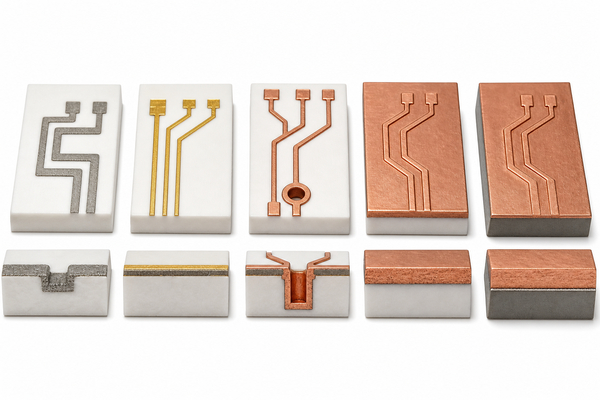
| Process | How the conductor is formed | Practical strength | Main limitation |
|---|---|---|---|
| Thick film | Conductive paste is screen-printed, dried and fired | Printed conductors, resistors and heaters with economical repeat production | Wider geometry and higher conductor resistivity than pure copper |
| Thin film | Adhesion and conductor layers are vacuum-deposited, then patterned by photolithography | Fine lines, smooth surfaces, precision resistors and RF structures | Thin metal carries limited current unless reinforced |
| DPC | A sputtered seed layer is patterned and copper is electroplated | Fine copper geometry, plated vias and controlled copper build | Copper thickness and panel stress must stay within the qualified process window |
| DBC | Copper foil is bonded directly to ceramic at high temperature and then etched | Heavy copper, high current and strong heat spreading | Etch geometry becomes less favorable as copper gets thicker |
| AMB | Copper is joined to ceramic with an active braze alloy | Strong interface and high thermal-cycle reliability, especially with silicon nitride | More process steps and cost than conventional DBC |
| HTCC/LTCC | Metal paste is printed on green ceramic layers and co-fired | Multilayer interconnects, buried conductors and hermetic packages | Material system and shrinkage rules are specialized |
HTCC and LTCC solve multilayer packaging problems, while thick film, thin film, DPC, DBC and AMB are the more common choices for planar ceramic circuit boards and power substrates.
How Do DBC, DPC, AMB, Thick Film and Thin Film Compare?
Use the most restrictive requirement to eliminate unsuitable processes. Current and copper thickness usually separate DBC/AMB from film processes; fine geometry and surface quality separate thin film/DPC from DBC and thick film.
| Selection factor | Thick film | Thin film | DPC | DBC | AMB |
|---|---|---|---|---|---|
| Conductor form | Fired metal paste | Deposited metal, optionally plated | Electroplated copper on a seed layer | Bonded copper foil | Brazed copper foil |
| Common conductor class | About 8-25 um per fired print | Submicron seed to several microns; thicker where plated | Commonly tens of microns, process dependent | Commonly 0.2-0.6 mm copper | Commonly 0.2-0.8 mm copper |
| Geometry | Moderate | Finest | Fine | Moderate to coarse as copper thickens | Moderate to coarse as copper thickens |
| Current capacity | Low to moderate | Low unless plated | Moderate | High | High |
| Integrated resistors/heaters | Excellent | Excellent for precision films | Usually separate components or added process | Not inherent | Not inherent |
| RF suitability | Application dependent | Strong for fine, smooth RF structures | Strong when copper roughness and geometry are controlled | Used mainly for power rather than fine RF routing | Used mainly for power and reliability |
| Thermal-cycle robustness | Depends on paste and protection | Depends on film stack and adhesion layer | Depends on plated stress and interface quality | Proven for power modules | Strong choice for severe cycling and mechanical stress |
| Relative process cost | Low to medium | High | Medium to high | Medium | High |
| Typical applications | Sensors, heaters, hybrid circuits | RF modules, optical packages, precision networks | LEDs, laser submounts, compact power circuits | IGBT/MOSFET modules, converters, motor drives | EV traction, rail, industrial power modules |
The ranges are typical process classes, not universal design rules. Final capability changes with the substrate, panel size, metal stack, supplier equipment, feature layout and inspection criteria.
How Should Current and Copper Thickness Influence the Choice?
Start with an electrical and thermal estimate. Continuous current, pulse duration, conductor length, permissible voltage drop and cooling conditions determine the required cross-sectional area. A thick conductor does not automatically solve temperature rise if the trace necks down at a pad, the ceramic-to-heatsink interface is poor or heat cannot leave the assembly.
For low-current signal paths, sensors and printed functions, thick film or thin film may be sufficient. Thick film paste is physically substantial but has higher resistivity than pure copper, so resistance per length must be calculated from the fired sheet resistance and geometry. Thin film offers clean geometry but normally needs selective plating when current exceeds the capacity of the deposited layer.
DPC is useful when the design needs both plated copper and relatively fine features. It is often a good bridge between thin-film precision and heavy-copper power substrates. As plated copper gets thicker, however, internal stress, sidewall shape, uniformity and ceramic flatness become more important.
DBC or AMB should enter the comparison when the circuit needs heavy copper for high current, heat spreading or power-semiconductor attachment. Copper thickness and ceramic thickness must be reviewed together because an unbalanced stack can bend, while thick copper around small ceramic islands can increase edge and corner stress.
How Do Line Width, RF Performance and Surface Finish Change the Selection?
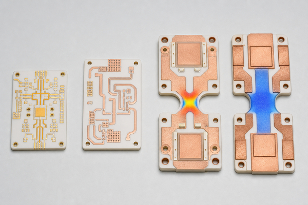
The minimum line and gap should be treated as production dimensions, not isolated prototype achievements. Thick film geometry is controlled by screen mesh, emulsion, paste rheology, printing and firing shrinkage. DBC and AMB geometry is constrained by copper thickness and etch undercut. Thin film and DPC use photolithography, so they are better starting points for dense layouts and smaller pads.
RF circuits add conductor roughness, edge definition, metal conductivity, substrate dielectric properties and thickness tolerance to the decision. Thin film is preferred for narrow transmission lines, filters and matching networks because vacuum deposition and lithography support smooth, repeatable geometry. DPC can also work for RF when the plated copper profile and finish are included in the electromagnetic model.
Surface finish must follow the assembly method. Bare copper may be suitable for controlled solder assembly and storage. Nickel/gold systems can protect copper and support soldering or wire bonding, but nickel thickness can add RF loss and every finish introduces another interface. Gold wire bonding, aluminum wire bonding, soldering and brazing should not share one generic finish requirement.
A thin film ceramic PCB for wireless communication illustrates the type of metallization selected when fine RF geometry and controlled bonding surfaces matter more than heavy copper.
How Should the Ceramic Material and Metallization Be Matched?
Metallization cannot be separated from the ceramic. Thermal conductivity, fracture toughness, surface finish, chemical behavior and coefficient of thermal expansion affect both performance and process yield.
| Ceramic substrate | Useful characteristics | Metallization implications |
|---|---|---|
| Alumina (Al2O3) | Economical, stable and widely available | Compatible with thick film, thin film, DPC and DBC; suitable when its thermal conductivity meets the heat-flow requirement |
| Aluminum nitride (AlN) | High thermal conductivity with electrical insulation | Used with DPC, DBC, AMB and film processes; surface preparation and moisture control require attention |
| Silicon nitride (Si3N4) | High fracture toughness and strong thermal-cycle performance | Commonly paired with AMB for demanding power modules; chosen for reliability rather than maximum thermal conductivity alone |
| Beryllium oxide (BeO) | Very high thermal conductivity | Handling and regulatory controls limit its use; alternative ceramics are usually evaluated first |
| Glass ceramic | Supports low-temperature co-firing and embedded multilayer functions | Metallization is part of the qualified LTCC material system and cannot be selected independently |
For example, AlN may reduce through-substrate thermal resistance, but it does not compensate for an undersized conductor or a poor die-attach interface. Silicon nitride can improve mechanical reliability, but the AMB braze layer and copper balance still control substrate behavior during cycling.
Which Reliability Risks Should Be Checked Before Selection?
Reliability failures usually begin at interfaces, corners or local geometry changes. The validation plan should target the expected failure mechanism instead of applying the same test list to every substrate.
| Risk | Typical cause | Selection or design response |
|---|---|---|
| Copper or film delamination | Inadequate surface preparation, weak adhesion layer, braze voids or contamination | Specify adhesion/peel criteria and inspect the relevant interface |
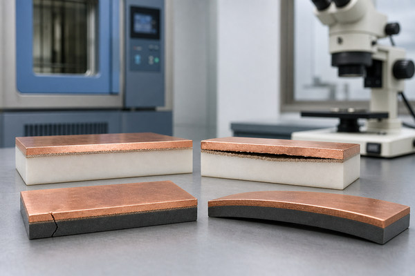
| Ceramic edge cracking | Heavy copper near the edge, sharp corners, poor singulation or assembly stress | Increase edge clearance, use radii and review copper balance |
| Bow and twist | Unequal copper coverage, one-sided metal or thermal history | Balance metal where possible and define flatness after processing |
| Trace overheating | Undersized conductor, high paste resistance, narrow necks or poor cooling | Calculate the complete current path and validate temperature rise |
| Electromigration or corrosion | Humidity, ionic contamination, silver migration or unsuitable protection | Select the conductor/finish for the voltage and environment |
| Solder or wire-bond failure | Wrong finish, roughness, thickness or contamination | Define the assembly method before selecting the final metal stack |
| Thermal-cycle cracking | CTE mismatch, brittle ceramic, interfacial voids or high local stress | Compare DBC and AMB, ceramic toughness and layout stress relief |
Thermal cycling, power cycling, high-temperature storage, humidity bias, peel testing, wire-pull testing and solder-shear testing are useful only when their conditions reflect the product's materials and operating profile.
How to Select Ceramic PCB Metallization by Application?
Industry names are only a starting point. Two products in the same market can need different metallization because their current, geometry, package and cooling path differ.
| Application condition | Practical first comparison | Why |
|---|---|---|
| Printed heater, resistor network or rugged sensor | Thick film vs thin film | Thick film integrates printed functions economically; thin film is justified by precision or stability |
| Fine RF or microwave network | Thin film vs DPC | Both support lithographic geometry; choose by metal thickness, surface and bonding requirements |
| LED or laser submount with fine routing | DPC vs thin film | DPC adds plated copper while retaining fine features; thin film favors the finest geometry and precision surfaces |
| Compact power converter | DPC vs DBC | DPC favors finer routing; DBC favors thicker copper and heat spreading |
| IGBT or MOSFET power module | DBC vs AMB | DBC is established for high current; AMB is favored when thermal cycling and mechanical reliability are more severe |
| EV traction or rail power module | AMB on Si3N4 vs qualified DBC stack | Tough ceramic and a strong brazed interface can justify AMB's additional cost |
| Multilayer RF package with embedded functions | LTCC vs HTCC | Co-fired systems address buried conductors, vias and hermetic packaging |
For fine copper routing, a DPC ceramic circuit board for laser equipment is a relevant process example. For thick copper in a power-semiconductor path, a DBC ceramic substrate for an IGBT module shows the different design priority. These examples should guide process comparison, not replace calculations for the actual stack.
What Data Should Be Confirmed Before Prototyping?
A useful prototype package makes the selection constraints explicit. Include the ceramic material and thickness, finished dimensions, conductor material and thickness, minimum line/space, copper balance, via construction, edge clearance and flatness requirement.
Also define the assembly interface: die attach or component solder alloy, reflow or brazing temperature, wire material and diameter, pad finish, heatsink attachment and cleaning method. Electrical inputs should include continuous and peak current, operating voltage, isolation requirement, allowable voltage drop and frequency range.
Reliability conditions should state the operating temperature range, thermal or power-cycle profile, humidity exposure, mechanical loading and acceptance tests. Mark critical dimensions and performance limits on the drawing. Avoid applying the tightest tolerance to every feature, because unnecessary precision can force a more complex metallization process without improving function.
FAQ
What is ceramic PCB metallization?
Ceramic PCB metallization is the process of attaching and patterning conductive metal on an insulating ceramic substrate. It forms traces, pads, vias and die-attach areas while providing an interface for assembly.
Which metallization is best for a ceramic PCB?
There is no universal best process. Thick film suits printed functions and moderate geometry, thin film suits precision and RF, DPC suits fine plated copper, DBC suits heavy-copper power circuits, and AMB suits demanding thermal cycling.
What is the difference between DPC and DBC ceramic PCB?
DPC builds copper by plating on a deposited seed layer and uses photolithography for fine patterns. DBC bonds copper foil directly to ceramic and then patterns it, providing thicker copper but less favorable fine-line capability.
What is the difference between DBC and AMB?
DBC bonds copper through a high-temperature copper-oxygen process. AMB uses an active braze alloy that reacts with the ceramic. AMB is commonly selected with silicon nitride when interface strength and thermal-cycle reliability justify the additional processing.
Is thick film metallization the same as thick copper?
No. Thick film refers to a printed-and-fired paste process. Its conductor may be thicker than a deposited thin film, but it is not equivalent to the heavy pure-copper foil used in DBC or AMB.
Can thin film ceramic circuits carry high current?
An unreinforced thin film has limited current capacity. Selective electroplating can increase conductor thickness, but if heavy copper is the primary requirement, DPC, DBC or AMB is usually a better comparison.
Which ceramic metallization is best for RF?
Thin film is a common first choice because it supports fine lines, smooth surfaces and controlled geometry. DPC can also be suitable when the design needs thicker copper, provided roughness, plating profile and finish are included in the RF model.
Which process is best for high-power modules?
DBC and AMB are the main candidates for heavy-copper power modules. DBC is widely used for established power stacks, while AMB on silicon nitride is often considered for severe thermal cycling and mechanical reliability.
Does aluminum nitride require a specific metallization?
Aluminum nitride can be used with thin film, thick film, DPC, DBC or AMB when the process is qualified for AlN. Surface preparation, oxidation behavior, moisture sensitivity and the selected interface chemistry must be controlled.
What causes metallization to peel from ceramic?
Common causes include contamination, inadequate surface preparation, an unsuitable adhesion layer, braze voids, excessive plated stress, thermal mismatch and assembly temperatures outside the qualified process window.
Should surface finish be chosen before metallization?
The assembly method should be known before the complete metal stack is finalized. Wire bonding, soldering and brazing have different requirements for finish material, thickness, roughness and cleanliness.
How can ceramic PCB metallization cost be controlled?
Use the least complex process that meets current, geometry, assembly and reliability limits. Avoid unnecessary copper thickness, blanket fine tolerances, premium finishes on noncritical areas and a high-reliability process when the operating profile does not require it.
Conclusion
How to Select Ceramic PCB Metallization is ultimately a stack decision. Use thick film for economical printed functions, thin film for fine and precise surfaces, DPC for fine plated copper, DBC for heavy-copper power paths, and AMB when severe cycling demands a stronger ceramic-metal system. Confirm the conductor, substrate, assembly and reliability requirements together before committing the layout.
BSTCeramicPCB can review the ceramic material, metallization process, copper balance, critical geometry and prototype validation plan. For technical support, contact sales@bstceramicpcb.com.
 Products
 About us
 Contact us



