






















































 HOME
HOME

-

Ceramic PCB for Humanoid Robot joint actuators
2026 04,07 -
LTCC PCB Surprises: What Most People Miss
2025 12,09 -
Step-by-Step Guide to DPC PCB Design for Sensor Systems
2025 12,03 -
Ceramic PCBs Essential Benefits and Applications
2025 12,01 -
How Al2O3 DPC Ceramic Substrate PCB Enhances Heat Dissipation in Modern Electronics?
2025 11,28 -
How to Choose Between Ceramic, FR4, and Metal Core PCBs
2025 11,27 -
DPC Ceramic PCB Materials: Surprising Science Inside
2025 11,26 -
Wire bondable 2-layer Alumina substrates PCB | Bstceramic PCB
2025 09,22 -
Silicon Nitride Substrate, Silicon Nitride Ceramic Substrate Formula
2025 05,08 -
What is thick film ceramic PCB?
2023 08,02
Choosing Metallized Alumina Substrates for Ceramic Circuits
Metallized alumina substrates combine an electrically insulating aluminum oxide base with metal surfaces that carry current, accept components or form joining interfaces. The important distinction is how that metal is attached and what it must do. A fine-line microwave circuit, a thick-copper power module and a brazed ceramic seal need different metallization systems, even when all three use alumina.
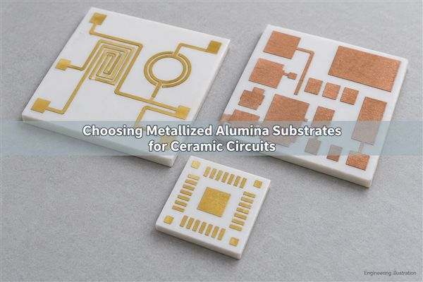
At BSTCeramicPCB, our ceramic circuit work includes plated copper, thin-film patterns and thick-film conductors. For circuit development, the useful starting point is the required conductor geometry and assembly method, followed by the ceramic grade and metal stack.
What Are Metallized Alumina Substrates?
A metallized substrate is a ceramic part with an intentionally bonded or deposited metal layer. Alumina, Al2O3, remains the insulating structural base; metallization creates conductive regions on its surface. Alumina is aluminum oxide, not aluminum metal, and a ceramic circuit board is not the same construction as an aluminum-core PCB.
Blank metallized sheets may have continuous metal on one or both faces. A finished alumina PCB has that metal patterned into traces, pads and isolated regions. Two metal-covered faces do not automatically provide electrical connections between them: those require defined vias or edge connections.
How Do Alumina Grade and Surface Condition Affect Metallization?
Ceramic grade and surface finish affect adhesion, film continuity and pattern accuracy. A 96% alumina grade is widely used for thick-film and copper-metallized circuits. Higher-purity grades, such as 99.6%, are also used for fine-feature electronic substrates, but purity alone does not specify roughness, flatness or dielectric behavior at the operating frequency.
For thin films, surface pits and contamination can interrupt narrow conductors or create weak interfaces. Our thin-film ceramic PCB capability includes a substrate roughness specification of Ra ≤0.1 µm, with Ra ≤0.05 µm listed for special needs. The appropriate finish must be matched to the selected material and circuit process; polishing every substrate to the tightest value is unnecessary for many thick-film designs.
Which Metallization Process Fits the Circuit?
Choose the process by conductor geometry, current demand and joining method. Metallized ceramic substrates are a broader category than copper-clad power substrates.
| Process | How the metal is formed | Where it fits | Main design constraint |
|---|---|---|---|
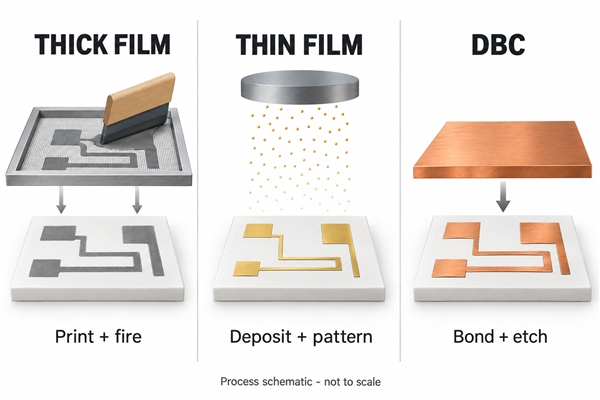
| Thick film | Conductive paste is printed and fired on ceramic | Hybrid circuits, resistor networks and patterned conductors | Paste compatibility, fired dimensions and repeated firing cycles |
| Thin film | Vacuum deposition creates a film that is patterned; plating may build thickness | Fine-pitch pads, RF circuits and precision structures | Surface quality, adhesion stack and lithographic pattern control |
| DPC, direct plated copper | A deposited conductive seed system supports electroplated copper | Patterned copper circuits and suitable metallized-via designs | Plating distribution, seed removal and hole geometry |
| DBC, direct bonded copper | Copper is bonded to ceramic through a controlled high-temperature copper-oxygen process | Thick-copper power circuitry | Etch undercut, conductor spacing and ceramic stress |
| Mo-Mn metallization | Molybdenum-manganese paste is fired; nickel plating commonly follows | Ceramic-to-metal brazed interfaces | Ceramic formulation, metallization firing and braze compatibility |
Active metal brazing is another ceramic-to-metal joining route. A reactive constituent in the braze enables bonding to ceramic, so it should not be described as simply another name for Mo-Mn metallization or DBC.
What Do the Layers in a Metal Stack Do?
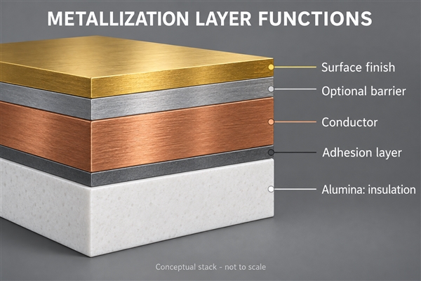
Different layers can provide adhesion, conduction, diffusion control and the final assembly surface. Naming only the visible top metal leaves important parts of the structure undefined.
For example, Cr Cu Au metallized alumina substrates use a chromium-copper-gold sequence: chromium supports adhesion to the ceramic, copper carries current, and gold provides the exposed surface. This is one established thin-film approach, not a universal stack for every temperature or assembly process. Whether an additional diffusion barrier is needed depends on the complete stack and thermal exposure.
Other designs use titanium or titanium-tungsten adhesion systems, platinum or nickel-containing barriers, and gold or another specified outer layer. The drawing should identify the layer order from ceramic outward. A nominal total metal thickness cannot establish the thickness or continuity of an individual barrier.
How Much Metal Thickness Is Needed?
Metal thickness must satisfy electrical resistance and assembly requirements without making patterning or thermal stress unnecessarily difficult. Conductor thickness and surface-finish thickness are separate specifications.
For a uniform conductor, resistance is approximately R = ρL/(wt), where ρ is resistivity, L is length, w is width and t is thickness. At unchanged material, length and width, doubling thickness approximately halves DC resistance. Fired pastes and very thin deposited films can differ from bulk-metal resistivity, so use the process-specific sheet resistance when available.
Our single-sided alumina DPC ceramic circuit board provides a concrete construction example: 96% Al2O3, a 1.0 ±0.1 mm ceramic base and 18 µm copper. These are specifications for that product, not a thickness prescription for every alumina circuit. A power layout may require much thicker copper; a fine-line RF layout may prioritize surface quality and controlled geometry instead.
How Are Circuit Patterns Formed Without Leaving Shorts?
Patterning must isolate the complete conductive stack, not just its thickest layer. In a plated-copper process, removing visible copper can leave a conductive seed or adhesion film between tracks. The removal sequence must clear that residual layer without damaging the retained conductors or ceramic surface.
For copper clad alumina, etch compensation also matters. Lateral etching narrows traces and increases the difference between artwork dimensions and final metal dimensions, especially with thicker copper. Define the finished conductor width, gap and edge position rather than treating the artwork as the final geometry.
Thin-film, thick-film and DBC design limits are not interchangeable. Minimum line width must be interpreted together with metal thickness, patterning method and tolerance. Verify narrow gaps electrically as well as optically; a nearly invisible conductive residue may not be obvious in an ordinary photograph.
How Do Double-Sided Circuits Connect Through Alumina?
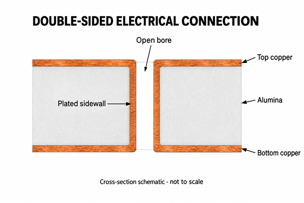
Double-sided metallized alumina requires an intentional interconnect, such as a plated hole, a qualified conductive fill or an edge-wrap conductor. The ceramic itself cannot carry the return current between two metal faces.
Hole formation and metallization must be planned together. Ceramic thickness, hole diameter, taper and sidewall quality influence whether a deposited seed and subsequent plating can form a continuous conductive path. A filled via is also not automatically a hermetic feedthrough; sealing performance requires its own construction and leak-test criteria.
For RF layouts, the distance and geometry of ground connections affect return-path inductance. For power layouts, evaluate the current-carrying cross-section and local heating at the via, rather than assuming a large surface pad guarantees a sufficiently robust connection.
Which Surface Finish Supports Soldering, Wire Bonding or Brazing?
Select the outer metal and underlying stack for the actual joining process. A gold-colored surface is not evidence that the substrate is suitable for every bond method.
| Assembly method | Required surface behavior | What to verify |
|---|---|---|
| Soldering | Reliable wetting without excessive loss of the conductor into solder | Solder alloy, finish thickness, barrier integrity and number of heat cycles |
| Gold wire bonding | Clean, bondable surface with a compatible underlying stack | Gold composition and thickness, pad roughness, bond process and pull/shear performance |
| Aluminum wire bonding | Surface compatible with the chosen wire and bonding conditions | Pad metallurgy and performance after the intended thermal exposure |
| Brazing | Wettable joining surface with a stable ceramic-metal interface | Metallization route, braze alloy, joint geometry and furnace cycle |
| Conductive adhesive attachment | Clean surface and stable electrical/mechanical contact after cure | Finish chemistry, adhesive compatibility and environmental aging |
For reflow assembly, measure the temperature at representative pads. The ceramic and metal can move heat away from the joint, while large and small metal areas respond differently. Increasing the oven setting alone does not establish a suitable solder profile.
Where Are These Substrates Used?
Metallized alumina serves applications where the circuit needs an insulating ceramic base plus a defined conductive or joining surface.
- LED modules: patterned copper distributes current and spreads heat beneath the emitter. Die-attach area and the thermal connection below the ceramic are part of the heat path.
- RF and microwave circuits: deposited conductors form transmission lines, matching networks and bonding pads. Ceramic thickness, dielectric properties, conductor geometry and ground continuity must be controlled together.
- Hybrid circuits and resistor networks: printed conductors can be combined with resistive elements and selected protective layers. Our thick-film high-density resistor circuit uses gold and silver-palladium pastes on its traces, illustrating why the conductor system must match the circuit function.
- Power modules: copper-metallized alumina supports isolated power circuitry. Copper pattern, ceramic thickness and thermal cycling affect the usable design, not simply the presence of a ceramic base.
- Ceramic-to-metal packages: localized metallization can provide a brazing interface for a frame or terminal. This is a joining application, distinct from fabricating the complete populated electronic package.
What Limits Thermal and Electrical Performance?
The assembled stack, rather than the alumina material name alone, determines thermal resistance and electrical isolation. Through the ceramic, a simple one-dimensional estimate is Rθ = t/(kA), with thickness t, thermal conductivity k and heat-transfer area A. Real assemblies also include spreading resistance, attachment layers and interfaces.
Thicker copper can spread heat laterally, but it does not change alumina's intrinsic thermal conductivity. If the ceramic layer dominates the temperature rise, reducing that layer's thickness or changing ceramic material may matter more than adding another copper increment. Mechanical handling strength and insulation requirements still constrain thinning.
Likewise, dielectric strength from a material datasheet is not the complete circuit voltage rating. Conductor spacing, exposed surface paths, edge geometry, contamination and the operating environment must be considered. Copper and alumina also expand differently during temperature cycling, concentrating stress near metal edges and attachment regions.
Which Defects Should Prototype Validation Target?
Validation should target the interfaces and features most likely to change during fabrication and assembly. A circuit that passes continuity before assembly can still develop pad lift, cracks or poor bonds after thermal processing.
| Observed problem | Possible mechanism | Relevant verification |
|---|---|---|
| Metal peeling or blistering | Surface contamination, weak adhesion or excessive stress | Process-appropriate adhesion test and inspection after thermal exposure |
| Leakage between traces | Residual seed metal, ionic contamination or insufficient separation | Insulation resistance and examination of the complete gap |
| Open or unstable via | Discontinuous sidewall metal or damaged fill | Continuity, cross-section and resistance change after cycling |
| Weak solder or wire bond | Unsuitable finish, contamination or assembly profile | Representative attachment trials and appropriate mechanical tests |
| Ceramic edge crack | Machining damage, clamping load or thermal mismatch | Edge inspection and testing in the actual mounting arrangement |
Agree the test method, specimen geometry and environmental conditions before comparing results. A peel measurement on thick copper is not directly equivalent to a stud-pull result on a small thin-film pad. The prototype should preserve the critical stack, smallest features and intended attachment cycle so it exercises the real design risks.
Matching the Metallization to the Circuit
The right metallized alumina substrates combine a suitable ceramic surface, a well-defined metal stack and geometry compatible with the intended assembly. Specify these together: thick copper does not solve every thermal problem, a gold finish does not guarantee bondability, and two metallized faces do not create a via.
For a plated-copper, thin-film or thick-film ceramic circuit, contact our BSTCeramicPCB team at sales@bstceramicpcb.com to discuss the metallization and assembly interface for your design.
 Products
 About us
 Contact us



